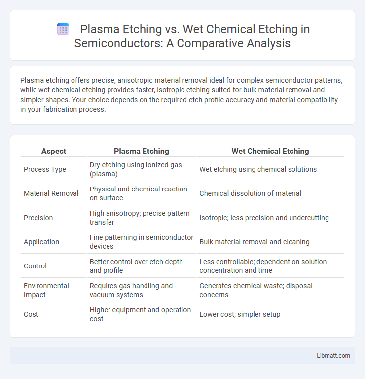
Plasma etching offers precise, anisotropic material removal ideal for complex semiconductor patterns, while wet chemical etching provides faster, isotropic etching suited for bulk material removal and simpler shapes. Your choice depends on the required etch profile accuracy and material compatibility in your fabrication process.
Table of Comparison
| Aspect | Plasma Etching | Wet Chemical Etching |
|---|---|---|
| Process Type | Dry etching using ionized gas (plasma) | Wet etching using chemical solutions |
| Material Removal | Physical and chemical reaction on surface | Chemical dissolution of material |
| Precision | High anisotropy; precise pattern transfer | Isotropic; less precision and undercutting |
| Application | Fine patterning in semiconductor devices | Bulk material removal and cleaning |
| Control | Better control over etch depth and profile | Less controllable; dependent on solution concentration and time |
| Environmental Impact | Requires gas handling and vacuum systems | Generates chemical waste; disposal concerns |
| Cost | Higher equipment and operation cost | Lower cost; simpler setup |
Introduction to Etching Techniques
Plasma etching uses ionized gases to selectively remove material from a substrate, offering precise control and anisotropic profiles essential for microfabrication. Wet chemical etching involves liquid chemicals that dissolve targeted layers, providing faster processing but often resulting in isotropic etch patterns. These etching techniques are critical in semiconductor manufacturing, MEMS fabrication, and nanoscale device engineering, where accuracy and surface integrity dictate device performance.
Defining Plasma Etching
Plasma etching is a precise, dry etching process that uses ionized gases to remove material from a substrate by chemically reacting with the surface, offering superior control and anisotropy compared to wet chemical etching. It enables fine pattern transfer in semiconductor manufacturing, microfabrication, and nanotechnology by selectively etching layers with minimal undercutting. Your choice between plasma etching and wet chemical etching depends on the required precision, material compatibility, and environmental safety considerations.
What is Wet Chemical Etching?
Wet chemical etching is a material removal process using liquid chemical solutions to selectively dissolve specific layers or features on a substrate, commonly employed in semiconductor manufacturing and microfabrication. This technique offers high selectivity and isotropic etching profiles, making it ideal for precise pattern transfer and surface treatment. Understanding your material's chemical compatibility is crucial for optimizing etch rates and achieving desired feature resolutions.
Process Mechanisms: Plasma vs Wet Etching
Plasma etching utilizes ionized gases to remove material through reactive ion bombardment and chemical reactions, providing precise anisotropic etch profiles essential for semiconductor device fabrication. Wet chemical etching relies on liquid chemical solutions to dissolve materials isotropically, often resulting in less directional control but faster material removal rates. The plasma process enables enhanced selectivity and surface smoothness compared to wet etching, which is more susceptible to undercutting and less compatibility with fine pattern transfer.
Material Compatibility and Selectivity
Plasma etching offers superior material selectivity and compatibility with a wide range of substrates, including metals, dielectrics, and semiconductors, due to its anisotropic, controllable, and dry process that minimizes undercutting. Wet chemical etching is generally less selective, often resulting in isotropic etching profiles and compatibility mainly with materials resistant to the specific chemical solutions used, limiting its use with multi-layered or delicate structures. The enhanced precision of plasma etching is critical for advanced semiconductor manufacturing where high aspect ratio features and precise pattern transfer are required.
Equipment and Operational Requirements
Plasma etching requires complex vacuum chambers, radio frequency power supplies, and precise gas flow control systems to generate reactive ions for material removal, demanding higher capital investment and maintenance. Wet chemical etching employs chemical baths and simple agitation setups, relying on selectivity of liquid reagents and temperature control, making it cost-effective but less precise for fine patterns. Both methods necessitate strict safety protocols, but plasma etching offers superior anisotropy and uniformity essential for advanced semiconductor fabrication.
Precision and Pattern Resolution Comparison
Plasma etching offers superior precision and higher pattern resolution compared to wet chemical etching, enabling finer feature sizes down to the nanometer scale crucial for advanced semiconductor fabrication. Wet chemical etching tends to produce isotropic etch profiles, resulting in lower resolution and less control over feature dimensions due to undercutting effects. Your choice between these techniques directly impacts the accuracy and quality of microfabrication processes, with plasma etching preferred for applications requiring exact pattern fidelity.
Environmental and Safety Considerations
Plasma etching generates fewer hazardous liquid wastes compared to wet chemical etching, reducing environmental contamination risks. It involves the use of reactive gases that can be safely contained and scrubbed, minimizing exposure to toxic chemicals and improving workplace safety. Wet chemical etching, relying on corrosive acids and bases, poses greater hazards due to chemical spills, toxic fumes, and complex waste disposal requirements, demanding stringent handling protocols.
Cost Factors and Scalability
Plasma etching generally involves higher initial equipment costs but offers greater precision and scalability for complex semiconductor fabrication compared to wet chemical etching. Wet chemical etching is typically lower in upfront expenses and suitable for simpler, low-volume applications, though its scalability is limited by chemical handling and disposal requirements. Cost efficiency in plasma etching improves significantly with large-scale production, while wet chemical etching remains more economical for small-batch processes.
Choosing the Right Etching Method
Choosing the right etching method depends on material compatibility, desired precision, and process control requirements. Plasma etching offers anisotropic profiles and superior control for microfabrication, making it ideal for semiconductor device patterning and delicate structures. Wet chemical etching provides cost-effective, isotropic removal suitable for bulk material processing but requires careful chemical selection to prevent damage and ensure uniformity.
Plasma Etching vs Wet Chemical Etching Infographic