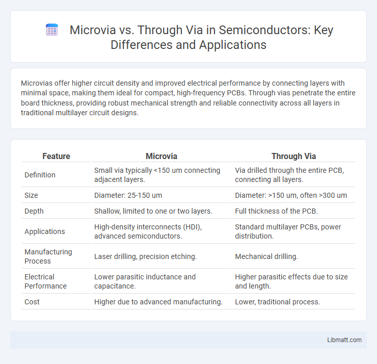
Microvias offer higher circuit density and improved electrical performance by connecting layers with minimal space, making them ideal for compact, high-frequency PCBs. Through vias penetrate the entire board thickness, providing robust mechanical strength and reliable connectivity across all layers in traditional multilayer circuit designs.
Table of Comparison
| Feature | Microvia | Through Via |
|---|---|---|
| Definition | Small via typically <150 um connecting adjacent layers. | Via drilled through the entire PCB, connecting all layers. |
| Size | Diameter: 25-150 um | Diameter: >150 um, often >300 um |
| Depth | Shallow, limited to one or two layers. | Full thickness of the PCB. |
| Applications | High-density interconnects (HDI), advanced semiconductors. | Standard multilayer PCBs, power distribution. |
| Manufacturing Process | Laser drilling, precision etching. | Mechanical drilling. |
| Electrical Performance | Lower parasitic inductance and capacitance. | Higher parasitic effects due to size and length. |
| Cost | Higher due to advanced manufacturing. | Lower, traditional process. |
Introduction to PCB Vias
Microvias are tiny, laser-drilled holes used in high-density printed circuit boards (PCBs) to create electrical connections between adjacent layers, enabling compact and complex designs. Through vias, in contrast, extend through the entire PCB thickness, connecting multiple layers but consuming more space and potentially affecting signal integrity. Your choice between microvia and through via impacts PCB manufacturing cost, signal performance, and overall board size.
Defining Microvia and Through Via
Microvia refers to a small, laser-drilled via used to connect layers in high-density printed circuit boards (PCBs), typically with a diameter less than 150 microns. Through via, on the other hand, extends through the entire PCB thickness, creating a conductive path across all layers. Understanding these differences ensures your PCB design optimizes space while maintaining reliable electrical connections.
Structural Differences
Microvias are small-diameter, laser-drilled holes that connect adjacent layers in a printed circuit board (PCB), typically less than 150 microns in diameter, enabling high-density interconnects. Through vias, on the other hand, pass through the entire PCB thickness, connecting all layers from top to bottom, with diameters usually exceeding 250 microns. The structural difference lies in microvias' limited depth and smaller size optimizing space and signal integrity, whereas through vias provide robust mechanical support but consume more board area.
Manufacturing Processes
Microvias are created using laser drilling, enabling precision and high-density interconnections in multilayer PCBs, while through vias are formed by mechanical drilling or laser, providing robust electrical connections from the top to the bottom layers. Microvias typically involve copper plating to fill the via, enhancing electrical performance and signal integrity for high-frequency applications. Through vias require more material removal and plating time due to their larger size, impacting manufacturing complexity and cost compared to microvias.
Electrical Performance
Microvias offer superior electrical performance due to their smaller size, which reduces signal path length and minimizes inductance and capacitance, resulting in lower signal loss and improved high-frequency signal integrity. Through vias, being larger and extending through the entire PCB, introduce higher parasitic inductance and capacitance, potentially causing signal reflections and degradation at high frequencies. Your electronic designs benefit from microvias when high-speed signal transmission and reduced electromagnetic interference are critical for optimal electrical performance.
Space and Density Considerations
Microvias occupy significantly less space compared to through vias, enabling higher circuit density and improved routing flexibility on printed circuit boards (PCBs). The smaller diameter and shallow depth of microvias reduce signal interference and allow for tighter component placement, critical in advanced high-density interconnect (HDI) designs. Through vias, extending through the entire PCB, consume more board area and limit miniaturization, making microvias essential for compact and multilayer PCB architectures.
Cost Comparison
Microvias typically incur higher manufacturing costs than through vias due to advanced drilling techniques like laser drilling and tighter manufacturing tolerances. Through vias are more cost-effective for standard PCB designs since mechanical drilling is faster and less expensive. Your choice depends on balancing budget constraints with design complexity, as microvias enable higher density and performance at a premium cost.
Reliability and Thermal Management
Microvias offer superior thermal management due to their smaller size and shorter electrical paths, reducing heat buildup and enhancing reliability in high-density PCB designs. Through vias, while easier to manufacture, can create higher thermal resistance and are more susceptible to stress-induced failures under thermal cycling. Enhanced heat dissipation and mechanical stability make microvias the preferred choice for applications demanding robust reliability and efficient thermal performance.
Typical Applications
Microvias are predominantly used in high-density interconnect (HDI) printed circuit boards (PCBs) for smartphones, tablets, and laptops where space-saving and signal integrity are critical. Through vias are common in standard multilayer PCBs for industrial equipment, automotive controls, and consumer electronics, offering reliable electrical connections across all layers. The choice between microvia and through via depends on factors like board complexity, signal frequency, and manufacturing cost constraints.
Choosing the Right Via for Your Design
Selecting between microvias and through vias depends on the PCB design's layer count, signal integrity requirements, and space constraints. Microvias offer reduced parasitic inductance and are ideal for high-density interconnects in multilayer boards, improving signal performance at high frequencies. Through vias provide robust mechanical connections for simpler, thicker boards but consume more space and may introduce signal degradation in high-speed designs.
Microvia vs Through Via Infographic