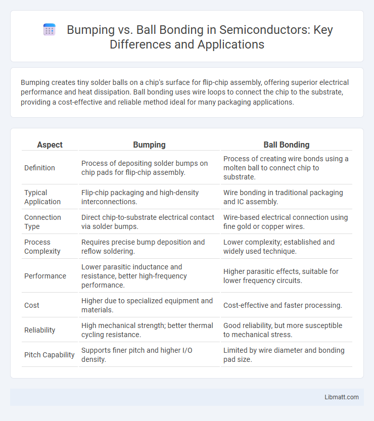
Bumping creates tiny solder balls on a chip's surface for flip-chip assembly, offering superior electrical performance and heat dissipation. Ball bonding uses wire loops to connect the chip to the substrate, providing a cost-effective and reliable method ideal for many packaging applications.
Table of Comparison
| Aspect | Bumping | Ball Bonding |
|---|---|---|
| Definition | Process of depositing solder bumps on chip pads for flip-chip assembly. | Process of creating wire bonds using a molten ball to connect chip to substrate. |
| Typical Application | Flip-chip packaging and high-density interconnections. | Wire bonding in traditional packaging and IC assembly. |
| Connection Type | Direct chip-to-substrate electrical contact via solder bumps. | Wire-based electrical connection using fine gold or copper wires. |
| Process Complexity | Requires precise bump deposition and reflow soldering. | Lower complexity; established and widely used technique. |
| Performance | Lower parasitic inductance and resistance, better high-frequency performance. | Higher parasitic effects, suitable for lower frequency circuits. |
| Cost | Higher due to specialized equipment and materials. | Cost-effective and faster processing. |
| Reliability | High mechanical strength; better thermal cycling resistance. | Good reliability, but more susceptible to mechanical stress. |
| Pitch Capability | Supports finer pitch and higher I/O density. | Limited by wire diameter and bonding pad size. |
Introduction to Semiconductor Packaging
Bumping and ball bonding are critical processes in semiconductor packaging that enable electrical connections between the chip and the substrate. Bumping involves depositing tiny solder bumps on the die pads, facilitating flip-chip attachments that offer superior signal transmission and thermal performance. Ball bonding uses fine wire loops, typically gold or copper, to connect the die to the package leads, providing reliable interconnects in wire-bonded packages.
Overview of Bumping and Ball Bonding
Bumping creates small solder bumps on a semiconductor wafer for flip-chip packaging, enhancing electrical connections and heat dissipation. Ball bonding uses tiny gold or copper spheres to connect the chip to the package leads through ultrasonic welding, commonly applied in wire bonding processes. Understanding the differences between bumping and ball bonding helps improve your microelectronics packaging strategy.
Key Differences Between Bumping and Ball Bonding
Bumping and ball bonding are critical processes in semiconductor packaging with distinct applications and techniques. Bumping involves creating solder bumps on chip pads to facilitate flip-chip connections, enhancing electrical performance and heat dissipation. Ball bonding, using a gold or copper wire to form a ball-shaped bond, is primarily employed for wire-to-chip or wire-to-lead connections, offering flexibility in complex circuit layouts.
Process Flow of Bumping Technology
The process flow of bumping technology involves wafer cleaning, photoresist application, and patterning through photolithography. Next, electroplating deposits metal bumps on designated pads, followed by photoresist stripping and wafer dicing into individual chips. This method enables enhanced electrical connection and mechanical stability in semiconductor packaging.
Process Flow of Ball Bonding Technology
Ball bonding technology initiates with the formation of a small molten solder ball on the wire tip, typically made of gold or copper, which is then pressed onto a bond pad to create the first bond. The process continues with the wire being looped and bonded again to the substrate or lead frame, forming a second bond point that ensures electrical connectivity. Your device's reliability depends on precise control of parameters such as temperature, ultrasonic power, and bonding force throughout this process flow to achieve optimal mechanical and electrical performance.
Materials Used in Bumping vs Ball Bonding
Bumping typically uses copper or solder as materials to create bumps on semiconductor wafers, providing robust electrical connections for flip chip packaging. Ball bonding employs gold, aluminum, or copper wires to form tiny balls that connect semiconductor die to lead frames, optimizing flexibility and conductivity. The choice of materials in both processes directly affects the mechanical strength, electrical performance, and thermal reliability of the final microelectronic assembly.
Applications of Bumping in Modern Electronics
Bumping plays a crucial role in modern electronics, especially in advanced semiconductor packaging techniques like flip-chip technology, where it enables high-density interconnections between the integrated circuit and the substrate. This process enhances electrical performance, reduces signal delay, and improves heat dissipation in devices such as microprocessors, memory chips, and system-on-chip (SoC) modules. Applications of bumping extend to mobile devices, high-performance computing, and automotive electronics, where reliability and miniaturization are critical.
Applications of Ball Bonding in Semiconductor Industry
Ball bonding is widely used in the semiconductor industry for creating reliable electrical connections between integrated circuits and their packages, especially in high-volume manufacturing of consumer electronics. This technique excels in applications requiring fine pitch interconnections and high-density packaging, such as microprocessors, memory chips, and sensors. Your devices benefit from ball bonding's ability to maintain connectivity under thermal and mechanical stress, ensuring long-term performance and reliability.
Advantages and Limitations of Each Method
Bumping offers advantages like improved electrical performance and miniaturization by enabling shorter interconnects and higher input/output density but faces limitations such as higher manufacturing complexity and cost. Ball bonding provides reliable mechanical and electrical connections with lower equipment expenses and well-established processes, though it struggles with scaling for ultra-fine pitch applications and may result in longer interconnect lengths. Choosing between bumping and ball bonding depends on application requirements including signal integrity, cost constraints, and package design complexity.
Future Trends in Bumping and Ball Bonding
Future trends in bumping and ball bonding emphasize advancements in miniaturization and material innovation to meet the demands of high-performance semiconductor devices. Emerging technologies such as laser bumping and ultrasonic ball bonding improve precision and reliability, catering to the growth of 5G, IoT, and automotive electronics. Your choice between these methods can significantly impact device efficiency and integration as the industry moves towards heterogeneous packaging and wafer-level solutions.
Bumping vs Ball Bonding Infographic