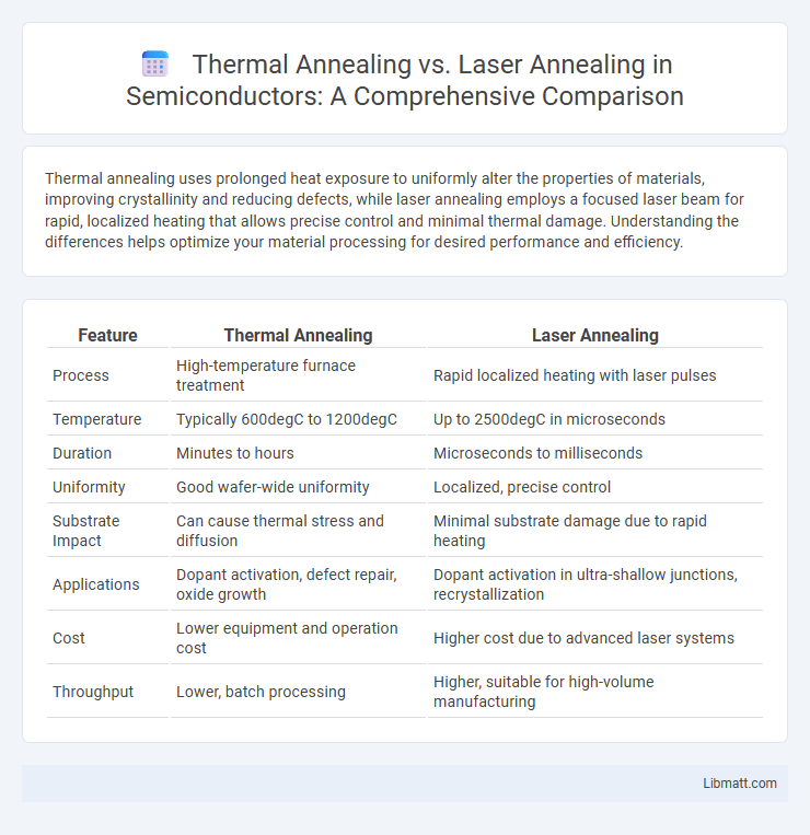
Thermal annealing uses prolonged heat exposure to uniformly alter the properties of materials, improving crystallinity and reducing defects, while laser annealing employs a focused laser beam for rapid, localized heating that allows precise control and minimal thermal damage. Understanding the differences helps optimize your material processing for desired performance and efficiency.
Table of Comparison
| Feature | Thermal Annealing | Laser Annealing |
|---|---|---|
| Process | High-temperature furnace treatment | Rapid localized heating with laser pulses |
| Temperature | Typically 600degC to 1200degC | Up to 2500degC in microseconds |
| Duration | Minutes to hours | Microseconds to milliseconds |
| Uniformity | Good wafer-wide uniformity | Localized, precise control |
| Substrate Impact | Can cause thermal stress and diffusion | Minimal substrate damage due to rapid heating |
| Applications | Dopant activation, defect repair, oxide growth | Dopant activation in ultra-shallow junctions, recrystallization |
| Cost | Lower equipment and operation cost | Higher cost due to advanced laser systems |
| Throughput | Lower, batch processing | Higher, suitable for high-volume manufacturing |
Introduction to Annealing Processes
Thermal annealing and laser annealing are essential techniques in semiconductor manufacturing that enhance material properties by relieving stress and improving crystalline structure. Thermal annealing involves heating the entire substrate uniformly at high temperatures to activate dopants and repair crystal defects, while laser annealing uses a focused laser beam for precise, rapid heating of localized regions, enabling ultra-fast dopant activation with minimal thermal budget. Your choice between these processes depends on specific fabrication requirements such as thermal sensitivity, dopant profiles, and desired material characteristics.
Fundamentals of Thermal Annealing
Thermal annealing involves heating a material to a specific temperature to alter its physical and chemical properties, such as reducing internal stresses or increasing ductility. This process facilitates atomic diffusion, enabling defect repair and recrystallization within the material's microstructure. Understanding the fundamentals of thermal annealing helps you optimize temperature and duration parameters for effective material treatment and improved performance.
Principles of Laser Annealing
Laser annealing uses high-intensity laser beams to rapidly heat the surface of a material, enabling localized recrystallization without affecting the substrate. This process allows precise control over temperature and duration, resulting in minimal thermal diffusion and enhanced material properties. Your materials benefit from improved electrical characteristics and reduced defects compared to traditional thermal annealing methods.
Key Differences Between Thermal and Laser Annealing
Thermal annealing and laser annealing differ primarily in heat application, precision, and speed; thermal annealing uses prolonged, uniform heating in a furnace, while laser annealing applies short, intense laser pulses for localized treatment. Thermal annealing is suited for bulk material softening and grain growth, whereas laser annealing enables precise control over surface properties without affecting the entire substrate. Your choice depends on the required process scale, material sensitivity, and desired microstructural changes.
Material Compatibility and Applications
Thermal annealing is widely compatible with bulk silicon wafers and various metals, making it ideal for traditional semiconductor manufacturing and metal alloy stress relief. Laser annealing offers precise energy delivery suitable for thin films, advanced semiconductor devices, and materials sensitive to high temperatures like amorphous silicon and flexible substrates. Your choice between thermal and laser annealing depends on material compatibility requirements and specific application needs in microelectronics or material science.
Process Efficiency and Time Comparison
Thermal annealing involves heating materials in a furnace over extended periods, often taking several hours to achieve uniform temperature and stress relief, while laser annealing uses highly focused laser beams to selectively heat and rapidly cool materials within seconds, significantly boosting process efficiency. Laser annealing provides precise control over localized areas, reducing thermal damage and minimizing processing time compared to the slower, bulk heating of thermal annealing. Choosing laser annealing can streamline your manufacturing workflow by drastically shortening cycle times while maintaining material integrity.
Temperature Control and Uniformity
Thermal annealing offers precise temperature control through gradual heating, ensuring uniform heat distribution across the entire substrate, which is critical for consistent material properties. Laser annealing, however, delivers rapid, localized heating with temperature spikes confined to targeted areas, allowing for high spatial resolution but potentially less uniformity over large surfaces. Your choice depends on whether uniform temperature control or localized precision is more crucial for your semiconductor or thin-film processing needs.
Cost Considerations and Scalability
Thermal annealing offers lower upfront equipment costs and easier scalability for large-scale production, making it a cost-effective option for bulk semiconductor manufacturing. Laser annealing, while presenting higher initial investment due to advanced laser systems, provides precise, localized treatment that can enhance device performance in smaller production runs or specialized applications. Your choice depends on balancing initial expenditure against scalability needs and the level of process control required for your specific manufacturing goals.
Impact on Material Properties
Thermal annealing improves material properties by uniformly heating the entire substrate, leading to reduced defects, enhanced crystallinity, and improved electrical conductivity in semiconductors. Laser annealing offers localized heating with rapid cooling, allowing precise control over dopant activation and minimal thermal damage to surrounding areas, which is critical for advanced microelectronics. Your choice between these methods depends on the desired material performance, balancing uniformity from thermal annealing against the spatial precision and speed of laser annealing.
Recent Advances and Future Trends
Recent advances in thermal annealing emphasize enhanced uniformity in temperature distribution and energy efficiency, using advanced furnace designs and optimized thermal profiles for semiconductor fabrication. Laser annealing breakthroughs focus on ultra-fast, localized heating with minimal thermal budget, enabling superior dopant activation and reduced diffusion for next-generation nanoelectronics. Future trends target hybrid methods combining thermal and laser annealing to balance throughput and precision, supported by AI-driven process control and real-time monitoring technologies.
Thermal Annealing vs Laser Annealing Infographic