Low-K dielectrics feature a lower dielectric constant, reducing parasitic capacitance and improving signal speed in microelectronic devices, while high-K dielectrics provide better insulation and higher capacitance, essential for advanced transistor gate stacks. Your choice between low-K and high-K dielectrics depends on the specific application requirements, balancing speed, power consumption, and device scaling.
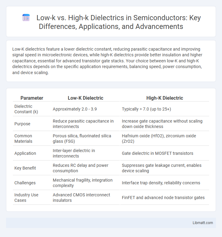
Table of Comparison
| Parameter | Low-K Dielectric | High-K Dielectric |
|---|---|---|
| Dielectric Constant (k) | Approximately 2.0 - 3.9 | Typically > 7.0 (up to 25+) |
| Purpose | Reduce parasitic capacitance in interconnects | Increase gate capacitance without scaling down oxide thickness |
| Common Materials | Porous silica, fluorinated silica glass (FSG) | Hafnium oxide (HfO2), zirconium oxide (ZrO2) |
| Application | Inter-layer dielectric in interconnects | Gate dielectric in MOSFET transistors |
| Key Benefit | Reduces RC delay and power consumption | Suppresses gate leakage current, enables device scaling |
| Challenges | Mechanical fragility, integration complexity | Interface trap density, reliability concerns |
| Industry Use Cases | Advanced CMOS interconnect insulators | FinFET and advanced node transistor gates |
Introduction to Dielectric Materials
Dielectric materials are essential insulators used to separate conductive layers in semiconductor devices, impacting device performance and reliability. Low-K dielectrics, with a dielectric constant less than that of silicon dioxide (approximately 3.9), reduce capacitive coupling and signal delay, making them ideal for advanced integrated circuits. High-K dielectrics have dielectric constants significantly higher than silicon dioxide, enhancing gate capacitance in transistors, which improves transistor scaling and power efficiency, critical for modern microprocessors and memory devices.
Defining Low-K and High-K Dielectrics
Low-K dielectrics have a dielectric constant typically below 3.9, minimizing parasitic capacitance and enhancing signal speed in semiconductor devices. High-K dielectrics possess a dielectric constant greater than 10, allowing for increased capacitance and better performance in advanced transistors, ensuring your electronic components operate efficiently in high-performance applications.
Material Properties and Structure
Low-K dielectrics possess a porous structure and low permittivity values, typically below 3.0, which minimize capacitive coupling and reduce signal delay in semiconductor devices. High-K dielectrics feature dense, high-permittivity materials such as hafnium oxide (HfO2) or zirconium oxide (ZrO2), enhancing gate capacitance and enabling further transistor scaling. Understanding these material properties and structures helps you optimize performance and power efficiency in integrated circuits.
Applications in Semiconductor Technology
Low-K dielectrics are essential in semiconductor technology for reducing parasitic capacitance in interconnects, improving signal speed and lowering power consumption in integrated circuits. High-K dielectrics, commonly used as gate insulators in advanced transistors, enable scaling of device dimensions while maintaining strong gate control and minimizing leakage currents. Choosing the appropriate dielectric material directly impacts your semiconductor device's performance, reliability, and energy efficiency.
Electrical Performance Comparison
Low-K dielectrics exhibit reduced capacitance, which minimizes parasitic capacitance and enhances signal speed in integrated circuits, benefiting high-frequency applications and reducing power consumption. High-K dielectrics provide superior gate control by increasing capacitance density without shrinking physical thickness, improving transistor drive current and reducing leakage currents in advanced CMOS technologies. The trade-off involves low-K materials favoring interconnect performance, while high-K materials optimize transistor switching characteristics for overall electrical efficiency.
Integration Challenges and Solutions
Low-k dielectric materials reduce capacitive coupling in semiconductor devices but face integration challenges such as poor thermal stability and mechanical strength, leading to film cracking and delamination during processing. High-k dielectrics offer better capacitance scaling but present issues with interface trap density and compatibility with existing silicon technology, affecting device performance and reliability. Solutions include advanced deposition techniques like atomic layer deposition (ALD) for uniform high-k films, and incorporating barrier layers or tailored low-k composites to enhance stability and integration in dual-damascene processes.
Impact on Device Scaling
Low-K dielectrics reduce parasitic capacitance between metal interconnects, enabling faster signal transmission and improved power efficiency in advanced semiconductor nodes. High-K dielectrics, with their higher dielectric constant, allow for physically thicker layers while maintaining equivalent capacitance, effectively suppressing gate leakage current and enhancing device control in ultra-scaled transistors. The choice between Low-K and High-K materials critically influences device scaling by balancing speed, power consumption, and leakage, directly impacting transistor performance and reliability in sub-10nm technology nodes.
Reliability and Longevity Factors
Low-K dielectrics offer improved reliability in semiconductor devices by reducing capacitance and minimizing signal delay, which lowers power consumption and heat generation, thus enhancing longevity. High-K dielectrics provide superior insulation and prevent leakage currents, contributing to device stability and extended operational life under high electric fields. Your choice between Low-K and High-K materials directly impacts the durability and reliability of electronic components in advanced integrated circuits.
Recent Advances in Dielectric Research
Recent advances in dielectric research have emphasized the development of ultra-low-k materials that reduce capacitance and improve signal speed in semiconductor devices, enabling higher performance and lower power consumption. High-k dielectrics, such as hafnium oxide (HfO2), continue to evolve with improved thermal stability and reduced leakage currents, facilitating further scaling in transistor gate insulators. Innovations in atomic layer deposition (ALD) and molecular engineering have enhanced the uniformity and interface quality of both low-k and high-k dielectrics, driving the next generation of nanoscale electronics.
Future Trends in Dielectric Development
Future trends in dielectric development emphasize the integration of ultra-low-K materials with enhanced mechanical stability to minimize parasitic capacitance in advanced semiconductor nodes. High-K dielectrics continue evolving through novel high-permittivity compounds like hafnium oxynitride that enable further scaling of transistor gate dielectrics while maintaining low leakage currents. Emerging research explores hybrid dielectric stacks combining low-K and high-K layers to balance dielectric constant, thermal stability, and process compatibility for next-generation microelectronics.
Low-K vs High-K Dielectric Infographic