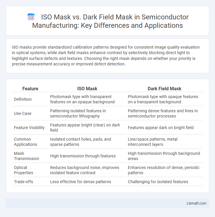
ISO masks provide standardized calibration patterns designed for consistent image quality evaluation in optical systems, while dark field masks enhance contrast by selectively blocking direct light to highlight surface defects and textures. Choosing the right mask depends on whether your priority is precise measurement accuracy or improved defect detection.
Table of Comparison
| Feature | ISO Mask | Dark Field Mask |
|---|---|---|
| Definition | Photomask type with transparent features on an opaque background | Photomask type with opaque features on a transparent background |
| Use Case | Patterning isolated features in semiconductor lithography | Patterning dense features and lines in semiconductor processes |
| Feature Visibility | Features appear bright (clear) on dark field | Features appear dark on bright field |
| Common Applications | Isolated contact holes, pads, and sparse patterns | Line/space patterns, metal interconnect layers |
| Mask Transmission | High transmission through features | High transmission through background areas |
| Optical Properties | Reduces background noise, improves isolated feature contrast | Enhances resolution of dense, periodic patterns |
| Trade-offs | Less effective for dense patterns | Challenging for isolated features |
Introduction to Photomask Technologies
Photomask technologies are critical in semiconductor manufacturing, where ISO masks and Dark Field masks serve distinct roles in patterning wafers with precision. ISO masks feature transparent fields with opaque patterns, making them ideal for positive photoresist applications, while Dark Field masks have opaque fields with transparent patterns suited for negative photoresist processes. Understanding these mask types enhances lithography accuracy and device performance in integrated circuit fabrication.
Understanding ISO Masks
ISO masks are essential in photography for controlling exposure and contrast by selectively blocking or permitting light, improving image sharpness and detail in both bright and dark areas. Unlike dark field masks, which are primarily used in microscopy to enhance the visualization of transparent specimens by blocking direct illumination, ISO masks serve a broader function in optimizing sensor response to different light intensities. Understanding ISO masks helps you achieve precise exposure control and better image quality across various lighting conditions.
Exploring Dark Field Masks
Dark Field Masks enhance imaging contrast by selectively blocking scattered light, which improves visibility of defects and surface irregularities compared to ISO Masks that primarily control exposure levels. These masks use specialized materials and patterns to filter undesired light angles, optimizing inspection processes in semiconductor manufacturing and microscopy. Dark Field Masks enable precise defect detection by capturing only the scattered light, making them crucial for quality control and surface analysis applications.
Key Differences Between ISO and Dark Field Masks
ISO masks are designed for general surface inspection using direct illumination, capturing high-contrast images of surface defects by reflecting light evenly. Dark field masks utilize angled or oblique lighting to highlight edges and contours, making it easier to detect micro-scratches and minute surface irregularities. The key difference lies in their illumination techniques: ISO masks rely on uniform light reflection, while dark field masks emphasize scattered light to enhance defect visibility.
Application Areas for ISO Masks
ISO masks excel in semiconductor lithography, where precise pattern transfer onto silicon wafers is crucial for integrated circuit manufacturing. They enable accurate definition of micro-scale features in electronics, optimizing performance in microprocessors and memory devices. These masks also find application in photomask fabrication for microelectromechanical systems (MEMS) and advanced photonics.
Use Cases for Dark Field Masks
Dark Field Masks excel in applications requiring detailed surface defect detection and contamination analysis, such as semiconductor wafer inspection and microelectronic quality control. These masks enhance contrast by blocking direct light and capturing only scattered or diffracted light, making them ideal for identifying scratches, particles, and surface irregularities. Your inspection process benefits from improved sensitivity to subtle defects that are often missed by ISO Masks, especially in high-precision manufacturing environments.
Impact on Lithography Process
ISO masks enhance lithography precision by providing improved pattern fidelity and better control over exposure doses, resulting in higher resolution and reduced defects in semiconductor manufacturing. Dark field masks, primarily used for patterned wafer inspection, impact the lithography process by enabling detection of sub-wavelength defects and critical dimension variations without affecting the exposure itself. Utilizing ISO masks leads to optimized lithographic process windows, while dark field masks contribute to yield enhancement through precise defect identification and process monitoring.
Pros and Cons of ISO Masks
ISO masks provide precise isolation of specific materials or regions in an image, enabling targeted editing without affecting surrounding areas, which enhances workflow efficiency. However, their complexity can lead to increased processing time and may require advanced software knowledge, potentially limiting accessibility for beginners. Compared to Dark Field masks, ISO masks offer greater accuracy but at the cost of higher computational resources and learning curve.
Advantages and Limitations of Dark Field Masks
Dark Field Masks offer high contrast imaging by blocking direct light and allowing only scattered light to reach the sensor, making them ideal for detecting surface defects and fine textures. Their main limitation is reduced brightness, which can require longer exposure times or stronger illumination, impacting real-time processing capabilities. You benefit from enhanced defect visibility but must balance this with potential sensitivity to lighting conditions.
Choosing the Right Mask for Semiconductor Manufacturing
Selecting the right mask for semiconductor manufacturing depends on your specific lithography requirements and defect sensitivity. ISO Masks offer high precision with isotropic etching, ideal for fine pattern stability and minimal feature distortion, while Dark Field Masks excel in enhancing contrast using opaque features for clearer defect detection on complex wafers. Your choice impacts yield and process control, making it essential to align mask type with production goals and inspection techniques.
ISO Mask vs Dark Field Mask Infographic