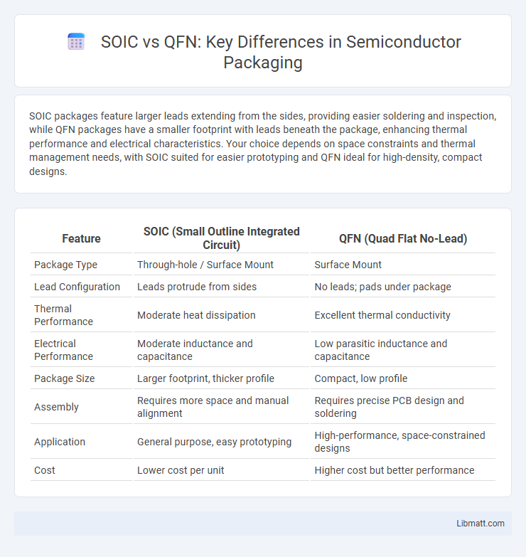
SOIC packages feature larger leads extending from the sides, providing easier soldering and inspection, while QFN packages have a smaller footprint with leads beneath the package, enhancing thermal performance and electrical characteristics. Your choice depends on space constraints and thermal management needs, with SOIC suited for easier prototyping and QFN ideal for high-density, compact designs.
Table of Comparison
| Feature | SOIC (Small Outline Integrated Circuit) | QFN (Quad Flat No-Lead) |
|---|---|---|
| Package Type | Through-hole / Surface Mount | Surface Mount |
| Lead Configuration | Leads protrude from sides | No leads; pads under package |
| Thermal Performance | Moderate heat dissipation | Excellent thermal conductivity |
| Electrical Performance | Moderate inductance and capacitance | Low parasitic inductance and capacitance |
| Package Size | Larger footprint, thicker profile | Compact, low profile |
| Assembly | Requires more space and manual alignment | Requires precise PCB design and soldering |
| Application | General purpose, easy prototyping | High-performance, space-constrained designs |
| Cost | Lower cost per unit | Higher cost but better performance |
Introduction to SOIC and QFN Packages
SOIC (Small Outline Integrated Circuit) and QFN (Quad Flat No-Lead) are two popular surface-mount packages used in electronic design. SOIC packages feature gull-wing leads extending from the package sides, making them easier to solder and inspect, whereas QFN packages have no leads and rely on pads underneath for electrical connections, offering a smaller footprint and improved thermal performance. Understanding these differences helps optimize your PCB layout for space, thermal management, and electrical performance.
Key Differences Between SOIC and QFN
SOIC (Small Outline Integrated Circuit) packages are larger with bent leads extending from the sides, allowing easier manual soldering and visual inspection, whereas QFN (Quad Flat No-Lead) packages are more compact, with leads underneath the package for better thermal performance and electrical grounding. You benefit from SOIC's straightforward handling in prototyping, while QFN offers superior high-frequency performance and reduced parasitic inductance in advanced designs. Key differences include form factor, lead configuration, thermal dissipation capabilities, and suitability for automated manufacturing processes.
Physical Dimensions and Footprint Comparison
SOIC (Small Outline Integrated Circuit) packages typically have a larger physical dimension and footprint compared to QFN (Quad Flat No-Lead) packages, which are designed for a more compact and low-profile surface mount assembly. The SOIC package features gull-wing leads extending from the sides, occupying more PCB space, whereas the QFN package has contacts beneath the chip, significantly reducing footprint and allowing higher component density on your board. Choosing QFN over SOIC can optimize space utilization, especially in applications demanding miniaturization and enhanced thermal performance.
Electrical Performance: SOIC vs QFN
QFN packages exhibit superior electrical performance compared to SOIC due to their shorter lead lengths and reduced parasitic inductance and resistance, enabling higher frequency operation and better signal integrity. SOIC packages have longer leads, which increase parasitic effects and electrical noise, making them less suitable for high-speed or RF applications. The low thermal resistance and improved heat dissipation of QFN further enhance its electrical stability under high power conditions.
Thermal Management in SOIC and QFN
The SOIC (Small Outline Integrated Circuit) package provides moderate thermal dissipation through its leads and exposed pads, but its thermal resistance is generally higher compared to QFN (Quad Flat No-lead) packages. QFN packages excel in thermal management due to their exposed thermal pad on the underside, which allows for efficient heat transfer to the PCB, significantly reducing junction temperature and improving reliability. Choosing QFN enhances your device's thermal performance, especially in high-power or compact applications where heat dissipation is critical.
Assembly and Soldering Considerations
SOIC packages offer through-hole or surface-mount assembly with visible leads, making manual soldering and inspection easier compared to QFN's leadless pads requiring precise reflow soldering and x-ray inspection. QFN assemblies provide better thermal performance and electrical characteristics but demand stringent PCB pad design and solder paste application to avoid voids and ensure reliable solder joints. Your choice between SOIC and QFN impacts soldering process complexity and inspection methods in manufacturing.
Reliability and Durability Factors
SOIC packages offer better mechanical robustness and ease of inspection, contributing to higher reliability in environments with mechanical stress or thermal cycling. QFN packages provide superior thermal performance and reduced inductance, enhancing durability in high-frequency and high-power applications. Your choice between SOIC and QFN should consider the operational conditions where mechanical strength or thermal efficiency impacts long-term device reliability.
Cost Implications: SOIC vs QFN
SOIC (Small Outline Integrated Circuit) packages generally have higher manufacturing and assembly costs compared to QFN (Quad Flat No-lead) due to larger lead frames and increased material use. QFN packages offer cost advantages by minimizing package size and lead length, which reduces substrate expenses and improves thermal performance, leading to lower overall system costs. The choice between SOIC and QFN directly impacts cost efficiency, especially in high-volume production where QFN's compact design can significantly reduce PCB footprint and assembly complexity.
Application Areas for SOIC and QFN Packages
SOIC packages excel in applications requiring easy inspection and manual soldering, commonly found in automotive control modules, consumer electronics, and industrial equipment due to their leaded design and accessibility. QFN packages suit high-performance, space-constrained environments such as smartphones, wearable devices, and wireless communication systems because of their low profile and excellent thermal and electrical performance. Understanding your project's size constraints and thermal requirements helps in selecting between SOIC's versatility and QFN's miniaturization benefits.
Choosing the Right Package: SOIC or QFN
Choosing the right package between SOIC and QFN depends on factors such as board space, thermal performance, and ease of assembly. SOIC packages offer larger leads for simpler soldering and inspection, making them suitable for prototyping and low-density layouts, while QFN packages provide a compact footprint with better thermal dissipation and electrical performance, ideal for high-frequency and space-constrained applications. Evaluating the specific requirements of the project, including mechanical robustness and manufacturing capabilities, ensures optimal package selection.
SOIC vs QFN Infographic