Surface passivation minimizes defects and recombination at the material's outer layer, enhancing electronic and optical performance by stabilizing the surface chemistry. Bulk passivation targets internal defects within the material, improving overall charge carrier lifetime and efficiency, which is critical for devices like solar cells and semiconductors.
Table of Comparison
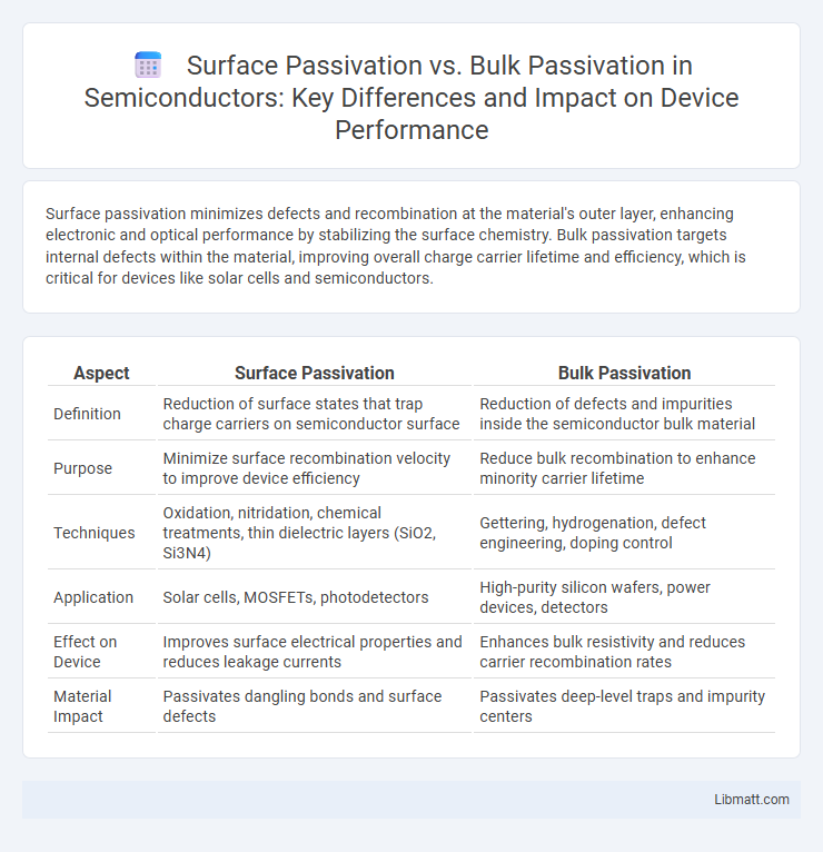
| Aspect | Surface Passivation | Bulk Passivation |
|---|---|---|
| Definition | Reduction of surface states that trap charge carriers on semiconductor surface | Reduction of defects and impurities inside the semiconductor bulk material |
| Purpose | Minimize surface recombination velocity to improve device efficiency | Reduce bulk recombination to enhance minority carrier lifetime |
| Techniques | Oxidation, nitridation, chemical treatments, thin dielectric layers (SiO2, Si3N4) | Gettering, hydrogenation, defect engineering, doping control |
| Application | Solar cells, MOSFETs, photodetectors | High-purity silicon wafers, power devices, detectors |
| Effect on Device | Improves surface electrical properties and reduces leakage currents | Enhances bulk resistivity and reduces carrier recombination rates |
| Material Impact | Passivates dangling bonds and surface defects | Passivates deep-level traps and impurity centers |
Introduction to Passivation in Materials Science
Passivation in materials science refers to the process of creating a protective layer on the surface or within the bulk of a material to enhance its resistance to corrosion and degradation. Surface passivation specifically targets the outermost layers, forming a thin oxide or nitride film that prevents environmental interaction, while bulk passivation involves modifying the internal structure or composition to mitigate defects and improve overall material stability. Both techniques are critical for extending the lifespan and performance of metals, semiconductors, and other advanced materials.
Defining Surface Passivation
Surface passivation involves creating a protective layer on the exterior of a semiconductor or material to reduce surface recombination and enhance electronic properties. This process typically utilizes thin oxide films, silicon nitride, or organic coatings to chemically stabilize dangling bonds and prevent environmental degradation. Effective surface passivation is crucial in improving device efficiency, especially in photovoltaic cells and semiconductor devices, by minimizing charge carrier losses at the material interface.
Understanding Bulk Passivation
Bulk passivation involves reducing recombination centers within the interior of a semiconductor material to improve charge carrier lifetime and overall device efficiency. This process minimizes defects such as vacancies or interstitial atoms in the bulk, enhancing the electrical properties of solar cells, transistors, or LEDs. Understanding bulk passivation is crucial for optimizing your semiconductor performance and achieving higher energy conversion rates.
Key Differences: Surface vs Bulk Passivation
Surface passivation targets the outer layer of a semiconductor, reducing surface defects and recombination sites to improve electronic performance, while bulk passivation focuses on minimizing defects and impurities within the material's interior. Surface passivation techniques often involve thin dielectric coatings or chemical treatments, whereas bulk passivation relies on doping or defect engineering within the crystal lattice. Understanding these key differences helps you optimize device efficiency by selecting the appropriate passivation method for specific applications.
Mechanisms Behind Surface Passivation
Surface passivation primarily involves creating a chemically stable layer on semiconductor material surfaces to reduce surface state densities and minimize charge carrier recombination. Techniques such as atomic layer deposition of aluminum oxide (Al2O3) provide fixed negative charges that repel minority carriers from the surface, enhancing electronic properties. This mechanism contrasts with bulk passivation, which targets defect reduction within the semiconductor volume rather than surface state mitigation.
Mechanisms Behind Bulk Passivation
Bulk passivation minimizes recombination by neutralizing defect states throughout the semiconductor's volume using impurity doping or hydrogenation techniques. This process enhances carrier lifetimes by saturating dangling bonds and filling deep-level traps within the bulk material. Your device performance improves as bulk passivation reduces charge carrier losses, leading to higher efficiency in applications like solar cells and electronic devices.
Impact on Electronic and Optical Properties
Surface passivation significantly reduces surface recombination velocities by eliminating dangling bonds, thereby enhancing carrier lifetime and improving photoluminescence efficiency in semiconductor materials. Bulk passivation targets defects within the crystal lattice, leading to decreased trap-assisted recombination and improved charge carrier mobility, which boosts both electronic conductivity and optical absorption. The combined optimization of surface and bulk passivation is critical for achieving high-performance optoelectronic devices with superior charge carrier dynamics and minimal energy loss.
Applications in Semiconductor and Photovoltaic Devices
Surface passivation significantly enhances semiconductor device performance by reducing surface recombination velocity, thereby increasing carrier lifetime and efficiency in photovoltaic cells and transistors. Bulk passivation targets defects and impurities within the semiconductor crystal lattice, improving volume recombination rates and enabling higher charge carrier mobility crucial for high-efficiency photovoltaic devices and advanced integrated circuits. Both passivation methods are essential in photovoltaic technology to maximize power conversion efficiency and in semiconductor manufacturing to optimize device reliability and longevity.
Challenges and Limitations of Each Approach
Surface passivation faces challenges in maintaining long-term chemical and environmental stability, often leading to degradation under operational stress and exposure to moisture or oxygen. Bulk passivation is limited by material compatibility and uniformity issues, as defects deep within the material can be difficult to effectively neutralize, impacting overall device performance. Both approaches struggle with scalability for large-area applications and require precise control to balance electronic properties without introducing new trap states.
Future Trends in Passivation Methods
Future trends in passivation methods emphasize nanotechnology and advanced materials to enhance both surface passivation and bulk passivation efficiency. Innovations in atomic layer deposition and organic-inorganic hybrid coatings improve defect passivation and stability at the microscopic level. Your ability to optimize semiconductor and photovoltaic device performance will benefit from these cutting-edge, scalable techniques.
Surface Passivation vs Bulk Passivation Infographic