Damascene steel features distinctive wavy patterns created through the layering and forging of different metals, offering both aesthetic appeal and enhanced strength compared to non-damascene steel. Your choice depends on whether you prioritize the unique craftsmanship and visual beauty of damascene or the simplicity and cost-effectiveness of non-damascene steel.
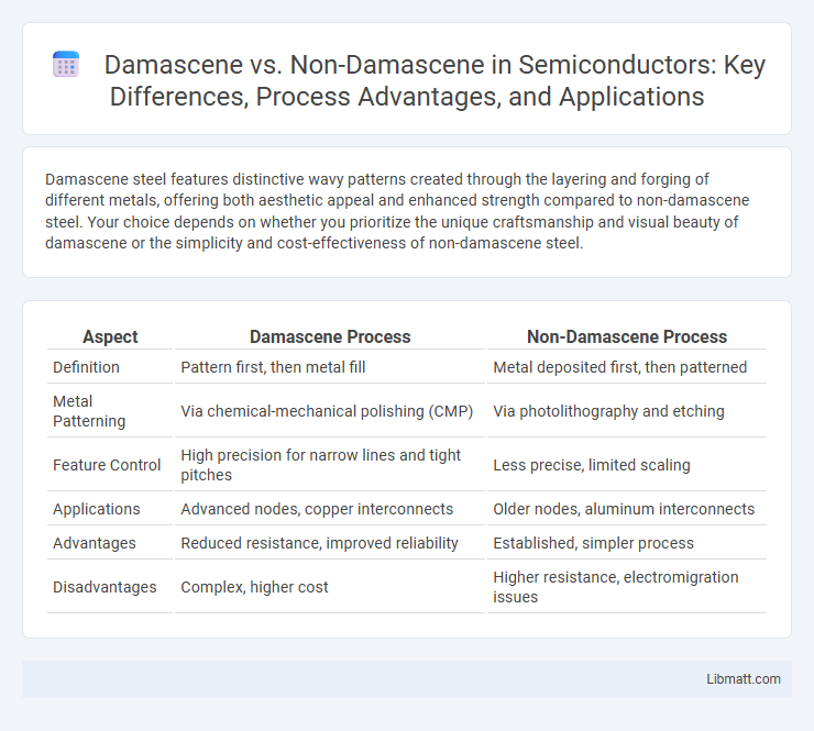
Table of Comparison
| Aspect | Damascene Process | Non-Damascene Process |
|---|---|---|
| Definition | Pattern first, then metal fill | Metal deposited first, then patterned |
| Metal Patterning | Via chemical-mechanical polishing (CMP) | Via photolithography and etching |
| Feature Control | High precision for narrow lines and tight pitches | Less precise, limited scaling |
| Applications | Advanced nodes, copper interconnects | Older nodes, aluminum interconnects |
| Advantages | Reduced resistance, improved reliability | Established, simpler process |
| Disadvantages | Complex, higher cost | Higher resistance, electromigration issues |
Introduction to Damascene and Non-Damascene Processes
Damascene and non-damascene processes are critical techniques in semiconductor fabrication, primarily used for creating metal interconnects on integrated circuits. The Damascene process involves etching trenches into the dielectric material and then filling them with metal, typically copper, which is polished to create a flat surface; this method offers superior conductivity and reduced resistance. Non-damascene processes often rely on subtractive etching of metal layers, which can lead to less efficient metal filling and increased challenges in achieving smooth interconnects, affecting the overall performance of your semiconductor devices.
Historical Evolution of Metallization Techniques
Damascene metallization techniques trace back to ancient Damascus, famous for its intricate sword-making using layered steel, influencing modern semiconductor interconnect processes by embedding metal within etched trenches. Non-damascene methods rely on subtractive etching, where metal layers are deposited first and then patterned by removal, a process dominant in earlier semiconductor manufacturing. Your understanding of semiconductor evolution benefits from recognizing how damascene's precision and scalability revolutionized metallization, enabling finer and more reliable circuit patterns compared to non-damascene approaches.
Fundamental Concepts: Damascene vs Non-Damascene
Damascene processes involve embedding metal features into pre-etched trenches on a substrate, ensuring planar surfaces essential for advanced semiconductor manufacturing. Non-damascene techniques typically rely on etching and deposition without trench filling, often resulting in less uniform surface topology. The Damascene approach enables higher metal density and improved electrical performance in integrated circuits compared to Non-damascene methods.
Process Flow: Damascene Method Explained
The Damascene method enhances semiconductor manufacturing by embedding metal interconnects directly into etched trenches on the wafer surface, followed by chemical-mechanical polishing to achieve a flat, smooth finish. This process flow contrasts with non-Damascene techniques, which typically involve depositing metal layers over the substrate and then etching them away to form circuits, often leading to less precise features and increased surface roughness. Your choice of the Damascene process optimizes device performance by ensuring superior planarity and reduced interconnect resistance, vital for advanced integrated circuits.
Process Flow: Non-Damascene Method Explained
The Non-Damascene method involves sequentially depositing and patterning metal layers without embedding copper in dielectric trenches, contrasting with the Damascene process where copper is inlaid into etched features. Its process flow includes metal deposition, photolithography, and etching steps directly on the dielectric surface, which can result in increased surface roughness and potential electromigration issues. This method is typically simpler but may face challenges in scaling for advanced semiconductor nodes due to its less effective copper integration and planarization capabilities.
Key Advantages of the Damascene Process
The Damascene process offers superior precision in creating intricate copper interconnects for semiconductor devices, enabling smaller feature sizes and higher circuit density compared to non-Damascene methods. Enhanced planarization achieved through Chemical Mechanical Polishing (CMP) in the Damascene process reduces defects and improves electrical performance by minimizing resistance and capacitance. This method also supports advanced packaging technologies by providing reliable and consistent copper wiring essential for high-speed, low-power integrated circuits.
Major Limitations of the Damascene Process
The major limitations of the Damascene process include complex fabrication steps that increase production time and cost, as well as challenges in achieving defect-free copper interconnects due to susceptibility to voids and seams. This process requires precise chemical-mechanical polishing (CMP), which can cause non-uniform metal thickness and surface roughness, impacting device reliability. Additionally, the Damascene method struggles with scalability for advanced nodes as copper diffusion barriers and low-k dielectrics present integration difficulties.
Comparative Analysis: Efficiency and Performance
Damascene technology offers superior efficiency and performance compared to non-damascene processes due to its precise copper interconnect fabrication, resulting in reduced resistance and enhanced signal integrity. Non-damascene methods typically rely on aluminum wiring, which exhibits higher resistivity and less reliability under high-frequency operations. Your choice between the two impacts overall device speed, power consumption, and thermal management, with damascene structures providing notable advantages in advanced integrated circuits.
Industrial Applications and Use Cases
Damascene technology excels in advanced semiconductor manufacturing, enabling the creation of ultra-thin metal interconnects with superior conductivity and reliability, crucial for high-performance microchips in consumer electronics and data centers. Non-damascene processes are typically used in less demanding applications where simpler metal layering suffices, such as in basic integrated circuits and automotive sensors. Understanding your specific industrial needs helps determine whether the precision and cost of damascene or the simplicity of non-damascene suits your production requirements.
Future Trends in Metallization Technologies
Future trends in metallization technologies emphasize the increasing adoption of Damascene processes due to their superior ability to create finer interconnects with reduced resistance and capacitance, crucial for advanced semiconductor nodes. Non-Damascene techniques, while simpler and cost-effective, struggle to meet the performance demands of next-generation integrated circuits as feature sizes shrink below 5 nanometers. Your choice of metallization technology will greatly impact the scalability and efficiency of chip manufacturing in the evolving landscape of high-performance electronics.
Damascene vs Non-damascene Infographic