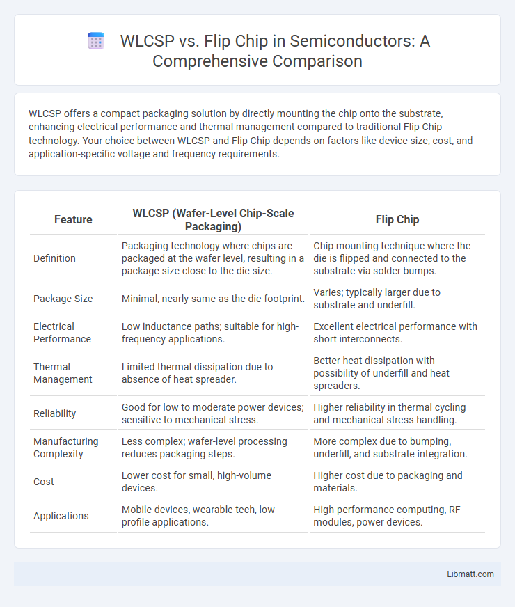
WLCSP offers a compact packaging solution by directly mounting the chip onto the substrate, enhancing electrical performance and thermal management compared to traditional Flip Chip technology. Your choice between WLCSP and Flip Chip depends on factors like device size, cost, and application-specific voltage and frequency requirements.
Table of Comparison
| Feature | WLCSP (Wafer-Level Chip-Scale Packaging) | Flip Chip |
|---|---|---|
| Definition | Packaging technology where chips are packaged at the wafer level, resulting in a package size close to the die size. | Chip mounting technique where the die is flipped and connected to the substrate via solder bumps. |
| Package Size | Minimal, nearly same as the die footprint. | Varies; typically larger due to substrate and underfill. |
| Electrical Performance | Low inductance paths; suitable for high-frequency applications. | Excellent electrical performance with short interconnects. |
| Thermal Management | Limited thermal dissipation due to absence of heat spreader. | Better heat dissipation with possibility of underfill and heat spreaders. |
| Reliability | Good for low to moderate power devices; sensitive to mechanical stress. | Higher reliability in thermal cycling and mechanical stress handling. |
| Manufacturing Complexity | Less complex; wafer-level processing reduces packaging steps. | More complex due to bumping, underfill, and substrate integration. |
| Cost | Lower cost for small, high-volume devices. | Higher cost due to packaging and materials. |
| Applications | Mobile devices, wearable tech, low-profile applications. | High-performance computing, RF modules, power devices. |
Introduction to WLCSP and Flip Chip Technologies
WLCSP (Wafer-Level Chip-Scale Packaging) and Flip Chip technologies represent advanced semiconductor packaging methods designed to enhance device performance and miniaturization. WLCSP involves directly packaging the die at the wafer level, enabling a compact footprint ideal for mobile and wearable applications. Flip Chip technology, by contrast, uses solder bumps to mount the chip face-down onto the substrate, providing superior electrical performance and heat dissipation, critical for high-frequency and high-power devices.
Key Differences Between WLCSP and Flip Chip
WLCSP (Wafer-Level Chip Scale Package) offers a compact form factor by packaging the die directly at the wafer level, resulting in reduced footprint and lower parasitic inductance compared to Flip Chip, which attaches the die to the substrate using solder bumps for improved electrical performance and heat dissipation. Flip Chip supports higher interconnect density and better heat management, making it suitable for high-performance applications, whereas WLCSP is favored for cost-sensitive, space-constrained devices. The choice between WLCSP and Flip Chip depends on factors such as device size, thermal requirements, and manufacturing complexity.
Design and Manufacturing Processes
WLCSP (Wafer-Level Chip Scale Package) involves directly packaging the semiconductor die at the wafer level, allowing for a smaller footprint and reduced manufacturing steps compared to traditional methods. Flip Chip technology attaches the die face-down onto the substrate using solder bumps, enabling higher interconnect density and improved electrical performance. Your choice between WLCSP and Flip Chip depends on design priorities such as miniaturization, thermal management, and production scalability.
Electrical Performance Comparison
WLCSP (Wafer-Level Chip-Scale Packaging) typically exhibits lower parasitic inductance and capacitance due to its minimal interconnection length, enhancing signal integrity and reducing signal delay compared to Flip Chip. Flip Chip packaging allows for direct electrical connections using solder bumps, which can provide superior thermal performance but may introduce higher parasitic effects affecting high-frequency electrical performance. Electrical performance in WLCSP generally favors applications requiring low inductance and high-speed signal transmission, while Flip Chip excels in power handling and heat dissipation capabilities.
Size and Form Factor Considerations
WLCSP (Wafer-Level Chip-Scale Packaging) offers a more compact size and minimal form factor by eliminating the traditional substrate, making it ideal for space-constrained applications. Flip Chip packaging, although slightly larger due to its added interposer or substrate, provides better electrical performance and thermal management for high-power devices. Your choice between WLCSP and Flip Chip depends on balancing the need for a small footprint with performance and heat dissipation requirements.
Cost Implications for WLCSP vs Flip Chip
WLCSP (Wafer-Level Chip Scale Package) typically offers lower overall packaging costs due to its streamlined manufacturing process and reduced substrate material usage, making it ideal for high-volume, cost-sensitive applications. Flip chip technology incurs higher initial investment in bumping and underfill materials, along with complex assembly steps, which can drive up costs especially in low to medium production volumes. Cost efficiency between WLCSP and flip chip is influenced by factors such as package size, thermal performance requirements, and production scale.
Reliability and Durability Factors
WLCSP (Wafer-Level Chip Scale Package) offers enhanced reliability through shorter interconnects and fewer solder joints, reducing failure points under mechanical stress compared to Flip Chip technology. Flip Chip excels in thermal dissipation and electrical performance but may face durability challenges due to CTE (Coefficient of Thermal Expansion) mismatches between the chip and substrate, leading to potential solder joint fatigue. Understanding these factors helps you select the packaging method that best meets your device's longevity and operational stability requirements.
Application Areas and Use Cases
WLCSP (Wafer-Level Chip-Scale Packaging) is widely used in compact mobile devices, wearable electronics, and IoT applications due to its small form factor and cost-efficiency, enabling high-density integration and improved electrical performance. Flip Chip technology is favored in high-performance computing, automotive sensors, and RF modules, where superior thermal management and higher input/output (I/O) density are critical. Your choice between WLCSP and Flip Chip should align with device size constraints, performance requirements, and application-specific demands.
Market Trends in WLCSP and Flip Chip Adoption
Market trends indicate a rising adoption of WLCSP (Wafer-Level Chip-Scale Packaging) driven by its compact size and improved electrical performance, making it ideal for smartphones and wearable devices. Flip Chip technology maintains strong demand in high-performance applications such as automotive electronics and data centers due to its superior thermal management and signal integrity. Understanding these trends can help you optimize your component selection for cost, size, and performance in emerging electronic markets.
Choosing the Right Packaging Technology
Choosing the right packaging technology between WLCSP (Wafer-Level Chip-Scale Package) and Flip Chip depends on factors like space constraints, electrical performance, and manufacturing costs. WLCSP offers a compact design ideal for mobile and small devices, optimizing your product's footprint and thermal management. Flip Chip provides superior electrical performance and reliability through direct die attachment, making it suitable for high-frequency and high-power applications.
WLCSP vs Flip Chip Infographic