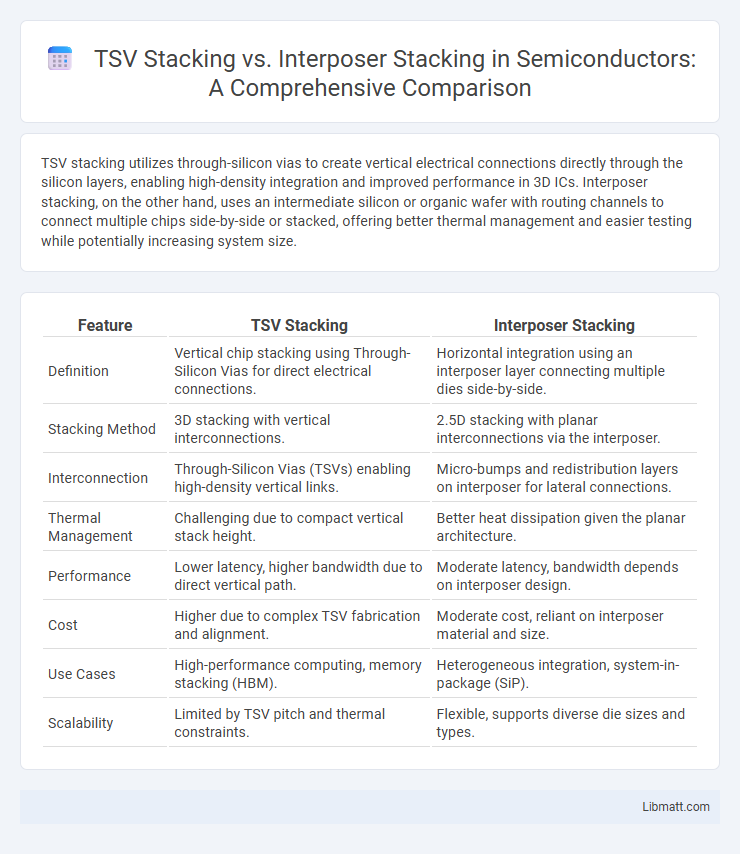
TSV stacking utilizes through-silicon vias to create vertical electrical connections directly through the silicon layers, enabling high-density integration and improved performance in 3D ICs. Interposer stacking, on the other hand, uses an intermediate silicon or organic wafer with routing channels to connect multiple chips side-by-side or stacked, offering better thermal management and easier testing while potentially increasing system size.
Table of Comparison
| Feature | TSV Stacking | Interposer Stacking |
|---|---|---|
| Definition | Vertical chip stacking using Through-Silicon Vias for direct electrical connections. | Horizontal integration using an interposer layer connecting multiple dies side-by-side. |
| Stacking Method | 3D stacking with vertical interconnections. | 2.5D stacking with planar interconnections via the interposer. |
| Interconnection | Through-Silicon Vias (TSVs) enabling high-density vertical links. | Micro-bumps and redistribution layers on interposer for lateral connections. |
| Thermal Management | Challenging due to compact vertical stack height. | Better heat dissipation given the planar architecture. |
| Performance | Lower latency, higher bandwidth due to direct vertical path. | Moderate latency, bandwidth depends on interposer design. |
| Cost | Higher due to complex TSV fabrication and alignment. | Moderate cost, reliant on interposer material and size. |
| Use Cases | High-performance computing, memory stacking (HBM). | Heterogeneous integration, system-in-package (SiP). |
| Scalability | Limited by TSV pitch and thermal constraints. | Flexible, supports diverse die sizes and types. |
Introduction to Advanced 3D IC Integration Techniques
TSV stacking leverages through-silicon vias to create vertical electrical connections between stacked semiconductor dies, enabling higher device density and improved performance in 3D integrated circuits. Interposer stacking uses a passive silicon interposer layer to connect multiple dies laterally, facilitating heterogeneous integration with enhanced signal integrity and thermal management. Both techniques address the growing demand for advanced 3D IC integration by optimizing interconnect density and enabling complex system-in-package designs.
What is TSV Stacking?
TSV Stacking, or Through-Silicon Via stacking, refers to a 3D packaging technology that vertically connects stacked semiconductor dies using tiny vertical electrical conduits called through-silicon vias. These TSVs pass through the silicon substrate, enabling high-density interconnections, reduced signal delay, and improved power efficiency compared to traditional 2D layouts. TSV Stacking is crucial in advanced semiconductor design for applications demanding enhanced performance, miniaturization, and integration, such as in memory modules, processors, and heterogeneous systems.
Understanding Interposer Stacking
Interposer stacking integrates multiple semiconductor dies on a silicon or organic interposer, enabling high-density interconnects and improved electrical performance with reduced signal latency compared to traditional TSV stacking methods. This approach supports heterogeneous integration by allowing different types of chips, such as logic and memory, to be combined in a compact form factor while enhancing thermal management. The fine-pitch routing and increased bandwidth in interposer stacking make it a preferred solution for high-performance computing and advanced packaging applications.
Key Differences Between TSV and Interposer Stacking
TSV stacking uses through-silicon vias to vertically connect multiple die within a single package, enabling high-density, low-latency integration with reduced signal paths. Interposer stacking, on the other hand, relies on a silicon or organic interposer layer to horizontally connect dies side-by-side, providing excellent electrical isolation and thermal management. Your choice between TSV and interposer stacking depends on factors like integration density, signal integrity, and manufacturing complexity.
Performance Comparisons: TSV vs Interposer
TSV stacking offers superior vertical electrical performance due to shorter interconnect paths, resulting in lower latency and higher bandwidth compared to interposer stacking. Interposer stacking provides greater flexibility for heterogeneous integration and easier heat dissipation but may introduce higher parasitic capacitance and signal delay. Your choice depends on whether peak electrical performance with TSV or versatile integration with interposers best suits your design requirements.
Cost Implications of Each Stacking Method
TSV stacking involves through-silicon vias that create vertical electrical connections, typically resulting in higher manufacturing complexity and thus increased production costs compared to traditional packaging. Interposer stacking uses an intermediate layer to connect dies laterally, which can reduce individual chip complexity but introduces added expenses from the interposer material and assembly process. Cost implications for TSV stacking often include advanced lithography and wafer thinning steps, while interposer stacking demands investment in silicon or organic interposer fabrication and alignment accuracy, influencing overall semiconductor packaging expenses.
Signal Integrity and Electrical Performance
TSV stacking offers superior signal integrity due to its shorter vertical interconnects, reducing parasitic capacitance and inductance compared to interposer stacking, which relies on longer lateral routing. Electrical performance in TSV integration benefits from direct through-silicon vias enabling higher bandwidth and lower latency communication between dies. Your system's efficiency improves with TSV stacking by minimizing signal loss and enhancing overall speed, making it preferable for high-performance computing applications.
Thermal Management Challenges
TSV stacking faces significant thermal management challenges due to the dense vertical integration of chips, which restricts efficient heat dissipation and can lead to hotspots affecting performance and reliability. Interposer stacking offers improved thermal pathways by allowing horizontal spreading of heat through the interposer layer, aiding in more effective thermal management. Both methods require advanced cooling solutions, but interposer stacking generally provides better support for mitigating thermal issues in 3D integrated circuits.
Application Scenarios: When to Use TSV or Interposer
TSV stacking is ideal for high-performance computing and memory integration requiring low latency and high bandwidth, such as in 3D NAND flash or HBM memory modules. Interposer stacking suits complex heterogeneous integration of multiple chips, like combining logic and analog components in advanced system-on-chip (SoC) designs and high-frequency applications. Choosing between TSV and interposer depends on factors like signal integrity, thermal management, cost constraints, and the specific electrical and mechanical requirements of the target application.
Future Trends in 3D IC Stacking Technologies
TSV stacking leverages through-silicon vias to enable high-density vertical interconnections, while interposer stacking uses a silicon or organic interposer for lateral component integration, enhancing signal routing and thermal management. Future trends in 3D IC stacking technologies emphasize heterogeneous integration, combining multiple device types and materials to achieve superior performance, reduced form factors, and improved power efficiency. Advances in monolithic 3D integration and wafer-level stacking are expected to drive higher interconnect density and lower latency, pushing the boundaries of next-generation semiconductor architectures.
TSV Stacking vs Interposer Stacking Infographic