X-ray inspection provides detailed internal imaging by using high-energy radiation to detect defects and structural inconsistencies without damaging the sample. Acoustic microscopy utilizes high-frequency sound waves to create high-resolution images of material interfaces and subsurface features, allowing you to identify voids, delamination, and other imperfections in electronic components.
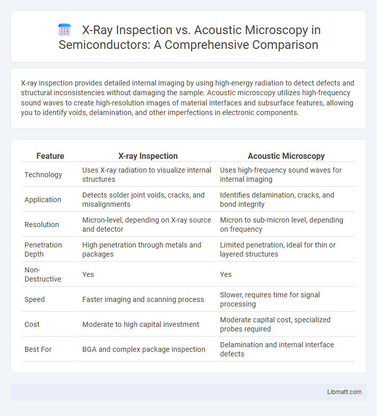
Table of Comparison
| Feature | X-ray Inspection | Acoustic Microscopy |
|---|---|---|
| Technology | Uses X-ray radiation to visualize internal structures | Uses high-frequency sound waves for internal imaging |
| Application | Detects solder joint voids, cracks, and misalignments | Identifies delamination, cracks, and bond integrity |
| Resolution | Micron-level, depending on X-ray source and detector | Micron to sub-micron level, depending on frequency |
| Penetration Depth | High penetration through metals and packages | Limited penetration, ideal for thin or layered structures |
| Non-Destructive | Yes | Yes |
| Speed | Faster imaging and scanning process | Slower, requires time for signal processing |
| Cost | Moderate to high capital investment | Moderate capital cost, specialized probes required |
| Best For | BGA and complex package inspection | Delamination and internal interface defects |
Introduction to Non-Destructive Testing Methods
X-ray inspection and acoustic microscopy are advanced non-destructive testing (NDT) methods used to evaluate the integrity of materials and components without causing damage. X-ray inspection utilizes high-energy radiation to penetrate and visualize internal structures, making it ideal for detecting cracks, voids, and inclusions in metals, composites, and electronics. Acoustic microscopy employs high-frequency sound waves to create detailed images of internal features, providing superior resolution for identifying delaminations, bond quality, and defects in thin layers and microelectronics, making it suitable for your quality control needs.
Understanding X-ray Inspection Technology
X-ray inspection technology uses high-energy radiation to penetrate materials and create detailed images of their internal structures, enabling precise defect detection in electronics and industrial products. This non-destructive method captures density variations and hidden flaws that are invisible to surface inspections, providing critical insights into solder joints, wire bonds, and component assemblies. Your quality control processes benefit from X-ray inspection's ability to reveal internal anomalies without damaging the tested object, unlike the surface-focused acoustic microscopy technique.
Principles of Acoustic Microscopy
Acoustic microscopy uses high-frequency ultrasonic waves to generate detailed images by detecting the reflection and transmission of sound waves within a material, enabling precise internal structural analysis. Unlike X-ray inspection, which relies on electromagnetic radiation to visualize density differences, acoustic microscopy provides superior resolution for detecting delaminations, voids, and material inconsistencies in soft and layered composites. This technique is essential for non-destructive testing in semiconductor, aerospace, and microelectronic industries where internal defect characterization at microscopic scales is critical.
Comparing Imaging Mechanisms: X-ray vs Acoustic
X-ray inspection uses high-energy electromagnetic radiation to penetrate materials and create images based on density variations, revealing internal structures with high resolution and contrast. Acoustic microscopy employs high-frequency ultrasonic waves to generate images by analyzing acoustic impedance differences within a specimen, offering detailed surface and subsurface information, especially for defects in layered materials. While X-ray excels in visualizing dense objects and volumetric features, acoustic microscopy provides superior sensitivity to material interfaces and mechanical properties.
Material Suitability and Application Areas
X-ray inspection excels in analyzing dense materials such as metals and complex assemblies, making it ideal for automotive, aerospace, and electronics industries for detecting internal defects like voids and cracks. Acoustic microscopy offers superior resolution for inspecting composite materials, polymers, and delicate semiconductor packages by detecting delamination, inclusions, and microstructural anomalies. Both techniques complement each other, with X-ray preferred for volumetric analysis and acoustic microscopy for high-resolution surface and subsurface evaluation.
Resolution and Defect Detection Capabilities
X-ray inspection offers high-resolution imaging capable of penetrating dense materials, making it effective for detecting internal defects such as voids, cracks, and solder joint issues in complex assemblies. Acoustic microscopy provides superior resolution at the micro-scale with its ultrasonic waves, excelling in identifying subsurface delaminations, voids, and bond integrity problems in thin and layered materials. Both technologies complement each other by addressing different types of defects and offering detailed insights into material integrity and structural quality.
Advantages of X-ray Inspection
X-ray inspection provides non-destructive analysis with high resolution, enabling precise detection of internal defects such as voids, cracks, and solder joint integrity in complex electronic assemblies. It offers faster inspection speeds and scalability for automated production environments compared to acoustic microscopy. The ability to visualize dense materials and layered structures without sample preparation makes X-ray inspection highly versatile across diverse industries including aerospace, automotive, and medical device manufacturing.
Benefits of Acoustic Microscopy
Acoustic microscopy offers superior subsurface imaging, enabling precise detection of internal defects such as delaminations, voids, and cracks that X-ray inspection may miss. Its ability to analyze material properties like elasticity and adhesion strength enhances quality control in complex electronic and composite structures. You benefit from non-destructive evaluation with higher resolution in layered materials, ensuring more reliable assessment of hidden flaws.
Limitations and Challenges of Each Method
X-ray inspection faces limitations in resolving fine structural details of complex multilayered electronic assemblies due to its reliance on density differences, which can obscure subtle defects within overlapping materials. Acoustic microscopy challenges include difficulty in detecting defects beneath highly attenuating or irregular surfaces, as well as sensitivity to coupling conditions and operator expertise. Choosing the appropriate method depends on your specific inspection requirements, balancing X-ray's penetration strength against acoustic microscopy's ability to reveal subsurface delaminations or voids.
Selecting the Right Technique for Your Application
X-ray inspection offers high-resolution imaging for detecting internal defects in dense materials, making it ideal for electronics and aerospace industries requiring non-destructive testing. Acoustic microscopy excels at identifying subsurface delaminations and voids in softer materials, providing detailed acoustic impedance maps crucial for semiconductor and composite material evaluation. Choosing the right technique depends on material type, defect nature, and required resolution, ensuring precise quality control and failure analysis.
X-ray Inspection vs Acoustic Microscopy Infographic