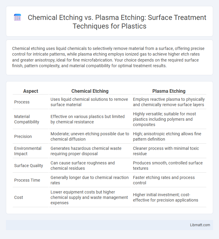
Chemical etching uses liquid chemicals to selectively remove material from a surface, offering precise control for intricate patterns, while plasma etching employs ionized gas to achieve higher etch rates and greater anisotropy, ideal for fine microfabrication. Your choice depends on the required surface finish, pattern complexity, and material compatibility for optimal treatment results.
Table of Comparison
| Aspect | Chemical Etching | Plasma Etching |
|---|---|---|
| Process | Uses liquid chemical solutions to remove surface material | Employs reactive plasma to physically and chemically remove surface layers |
| Material Compatibility | Effective on various plastics but limited by chemical resistance | Highly versatile; suitable for most plastics including polymers and composites |
| Precision | Moderate; uneven etching possible due to chemical diffusion | High; anisotropic etching allows fine pattern definition |
| Environmental Impact | Generates hazardous chemical waste requiring proper disposal | Cleaner process with minimal toxic residue |
| Surface Quality | Can cause surface roughness and chemical residues | Produces smooth, controlled surface textures |
| Process Time | Generally longer due to chemical reaction rates | Faster etching rates and process control |
| Cost | Lower equipment costs but higher chemical supply and waste management expenses | Higher initial investment; cost-effective for precision applications |
Introduction to Surface Treatment Techniques
Chemical etching employs liquid chemicals to selectively remove material from a surface, creating precise patterns or textures through controlled chemical reactions. Plasma etching utilizes ionized gases in a plasma state to physically and chemically sputter away surface layers, offering high precision and anisotropic etching capabilities. Both techniques are essential in microfabrication and surface treatment for enhancing material properties and achieving fine structural details.
Overview of Chemical Etching
Chemical etching is a precise surface treatment technique that uses acidic or alkaline chemical solutions to selectively remove material from a substrate, enabling intricate pattern creation and fine detail work. It offers high accuracy for metals, glass, and semiconductors, making it ideal for applications requiring fine microstructures or detailed surface modifications. Your choice of chemical etching ensures cost-effective processing with minimal mechanical stress, suitable for delicate components and complex designs.
Overview of Plasma Etching
Plasma etching employs ionized gases to precisely remove material from a substrate, offering superior control and anisotropic etching compared to chemical etching. This surface treatment technique enables high selectivity and uniformity, making it ideal for microfabrication and semiconductor applications. Your manufacturing process benefits from reduced chemical waste and enhanced pattern fidelity with plasma etching.
Mechanisms of Action: Chemical vs. Plasma Etching
Chemical etching relies on liquid chemical solutions to selectively dissolve the surface material through a controlled reaction, enabling precise material removal based on chemical reactivity. Plasma etching, on the other hand, uses ionized gases and reactive plasma species to physically and chemically bombard the surface, allowing for anisotropic etching and finer patterning. Understanding these distinct mechanisms of action can help you select the optimal etching process for your surface treatment needs.
Materials Compatibility and Applications
Chemical etching offers high compatibility with metals like copper, stainless steel, and aluminum, making it ideal for intricate patterns on circuit boards and decorative parts; it is less suitable for polymers and ceramics due to chemical reactions. Plasma etching excels with a broad range of materials, including semiconductors, polymers, and glass, enabling precise microfabrication and surface cleaning in electronics and nanotechnology. Applications of chemical etching focus on metal finishing and prototyping, whereas plasma etching is preferred in semiconductor device fabrication, microelectromechanical systems (MEMS), and advanced surface engineering.
Precision and Resolution Comparison
Chemical etching offers moderate precision with isotropic material removal, which can limit resolution due to undercutting effects. Plasma etching delivers higher precision and superior resolution through anisotropic etching, enabling finely detailed surface patterns with minimal lateral etching. Your choice between these methods should consider the required feature size and edge definition for optimal surface treatment results.
Environmental Impact and Safety Considerations
Chemical etching involves hazardous chemicals like acids and solvents that pose risks of toxic emissions, chemical spills, and hazardous waste disposal challenges, requiring stringent handling and safety measures. Plasma etching utilizes reactive gases and generates fewer harmful byproducts, offering a cleaner process with lower environmental impact and improved workplace safety. Both methods demand strict compliance with safety protocols, but plasma etching is generally considered the safer and more environmentally friendly option in surface treatment applications.
Process Speed and Scalability
Chemical etching offers a faster process speed due to its aggressive material removal rate, making it suitable for high-volume production with consistent results. Plasma etching, while generally slower, provides superior precision and uniformity, which can be scaled effectively for complex or delicate surface treatments in semiconductor manufacturing. Your choice depends on whether rapid throughput or fine control and scalability for intricate patterns are more critical for your application.
Cost Analysis: Chemical vs. Plasma Etching
Chemical etching generally offers a lower initial investment and operating cost compared to plasma etching, making it cost-effective for small-scale or low-precision surface treatments. Plasma etching, despite higher equipment and maintenance expenses, delivers greater precision and environmental benefits, potentially reducing long-term operational costs in high-volume or sensitive applications. Evaluating your project's scale and precision requirements can help determine which etching method provides the most cost-efficient surface treatment solution.
Choosing the Right Etching Method for Your Application
Selecting the optimal etching method depends on material type, precision requirements, and environmental considerations. Chemical etching offers high selectivity and smooth surface finishes ideal for complex patterns on metals and delicate substrates. Plasma etching provides superior anisotropy and cleaner process control, making it suitable for semiconductor fabrication and applications demanding fine feature resolution.
Chemical etching vs plasma etching (surface treatment) Infographic