2.5D integration offers improved performance and power efficiency by placing multiple chips side-by-side on an interposer, reducing signal delay compared to traditional packaging. Your choice between 2.5D and 3D integration should consider factors like thermal management, cost, and complexity, as 3D stacking allows for higher density and vertical interconnections but may face more heat dissipation challenges.
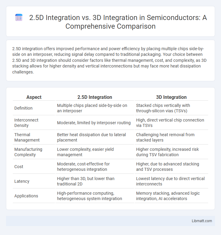
Table of Comparison
| Aspect | 2.5D Integration | 3D Integration |
|---|---|---|
| Definition | Multiple chips placed side-by-side on an interposer | Stacked chips vertically with through-silicon vias (TSVs) |
| Interconnect Density | Moderate, limited by interposer routing | High, direct vertical chip connection via TSVs |
| Thermal Management | Better heat dissipation due to lateral placement | Challenging heat removal from stacked layers |
| Manufacturing Complexity | Lower complexity, easier yield management | Higher complexity, increased risk during TSV fabrication |
| Cost | Moderate, cost-effective for heterogeneous integration | Higher, due to advanced stacking and TSV processes |
| Latency | Higher than 3D, but lower than traditional 2D | Lowest latency due to direct vertical interconnects |
| Applications | High-performance computing, heterogeneous system integration | Memory stacking, advanced logic integration, AI accelerators |
Introduction to 2.5D and 3D Integration
2.5D integration involves placing multiple dies side-by-side on an interposer, enabling improved performance and power efficiency compared to traditional 2D chip designs. 3D integration stacks chips vertically, offering higher density and shorter interconnects for enhanced speed and reduced latency. Understanding the differences helps you choose the optimal integration method for your semiconductor design needs.
Key Differences Between 2.5D and 3D Integration
2.5D integration stacks multiple chips side-by-side on an interposer, utilizing high-density interconnects for improved performance and power efficiency, while 3D integration involves vertically stacking active layers, enabling shorter interconnect distances and higher functional density. Thermal management is more challenging in 3D integration due to heat dissipation issues within the stacked layers, whereas 2.5D offers easier cooling by spreading components laterally. Your choice between 2.5D and 3D integration depends on factors like design complexity, cost, and targeted application performance requirements.
Architectural Design: 2.5D vs 3D Approaches
2.5D integration leverages a silicon interposer to place multiple dies side-by-side on a common substrate, enabling high-bandwidth communication while maintaining thermal and yield advantages. In contrast, 3D integration stacks dies vertically using through-silicon vias (TSVs), offering greater interconnect density and reduced latency but facing increased thermal management and manufacturing complexity challenges. The choice between 2.5D and 3D architectures depends on performance requirements, thermal constraints, and cost considerations in advanced semiconductor design.
Performance Comparison: Speed and Bandwidth
2.5D integration offers improved speed and bandwidth compared to traditional 2D designs by placing multiple dies side-by-side on a silicon interposer, reducing interconnect lengths and latency. 3D integration surpasses 2.5D by stacking dies vertically, enabling even shorter interconnects and higher bandwidth density due to through-silicon vias (TSVs), resulting in lower power consumption and faster data transfer rates. However, 3D integration faces thermal challenges that can impact performance, while 2.5D provides a more balanced trade-off between speed, bandwidth, and thermal management.
Power Consumption and Thermal Management
2.5D integration offers improved power consumption efficiency by enabling shorter interconnects and better signal routing compared to traditional packaging, though it generally exhibits higher power use than 3D integration due to longer inter-die distances. In contrast, 3D integration significantly reduces power consumption by stacking dies vertically, minimizing interconnect length and capacitance, but this approach poses greater challenges for thermal management because of increased power density and heat dissipation complexity within stacked layers. Effective thermal solutions such as microfluidic cooling or advanced heat spreaders are critical in 3D integrated circuits to manage hotspots and maintain reliability, while 2.5D platforms benefit from easier thermal dissipation through their lateral die placement.
Cost Analysis: Manufacturing and Scalability
2.5D integration offers a cost-effective manufacturing process by enabling independent optimization of each die before assembly, significantly reducing yield loss compared to monolithic 3D integration. The use of silicon interposers in 2.5D allows for easier scalability and integration of heterogeneous components without the complex thermal and stress issues typical in 3D stacking. In contrast, 3D integration involves higher fabrication costs related to through-silicon vias (TSVs) and complex wafer bonding, limiting its scalability despite benefits in performance and form factor.
Applications and Use Cases in Industry
2.5D integration is widely used in high-performance computing and networking applications where heterogeneous components like CPUs, GPUs, and memory are placed on an interposer to improve bandwidth and reduce latency without the thermal challenges of full 3D stacking. 3D integration is favored in mobile devices and advanced AI accelerators due to its ability to stack multiple layers of logic and memory vertically, achieving greater density and power efficiency in compact spaces. Industries such as data centers, automotive electronics, and consumer electronics selectively adopt these technologies to balance performance, cost, and thermal management based on specific workload and form factor requirements.
Integration Challenges and Technical Barriers
2.5D integration faces challenges such as interposer fabrication complexity, thermal management issues, and precise die-to-die alignment, whereas 3D integration encounters more severe technical barriers including through-silicon via (TSV) fabrication difficulties, increased heat dissipation demands, and higher mechanical stress within stacked dies. Both technologies struggle with signal integrity and yield optimization, but 3D integration's vertical stacking adds complexity in terms of thermal hotspots and TSV-induced reliability concerns. Advanced packaging techniques and materials innovation are critical to overcoming these inherent integration challenges in both 2.5D and 3D approaches.
Future Trends in Semiconductor Integration
2.5D integration offers enhanced performance and power efficiency by placing multiple dies side-by-side on an interposer, improving interconnect density and thermal management compared to traditional packaging. 3D integration, stacking dies vertically with through-silicon vias (TSVs), enables even higher integration density and reduced latency but faces challenges in heat dissipation and manufacturing complexity. Future trends indicate growing adoption of hybrid approaches combining 2.5D and 3D techniques, driven by the demand for miniaturization, heterogeneous integration, and advanced computing applications, shaping Your semiconductor solutions with scalable and efficient architectures.
Choosing Between 2.5D and 3D Integration
Choosing between 2.5D and 3D integration depends on your design complexity, thermal management, and cost constraints. 2.5D integration offers improved electrical performance and easier heat dissipation by placing multiple chips side-by-side on an interposer, making it ideal for moderate-density applications. In contrast, 3D integration stacks chips vertically, providing higher interconnect density and form factor reduction but requiring advanced thermal solutions and higher manufacturing costs.
2.5D Integration vs 3D Integration Infographic