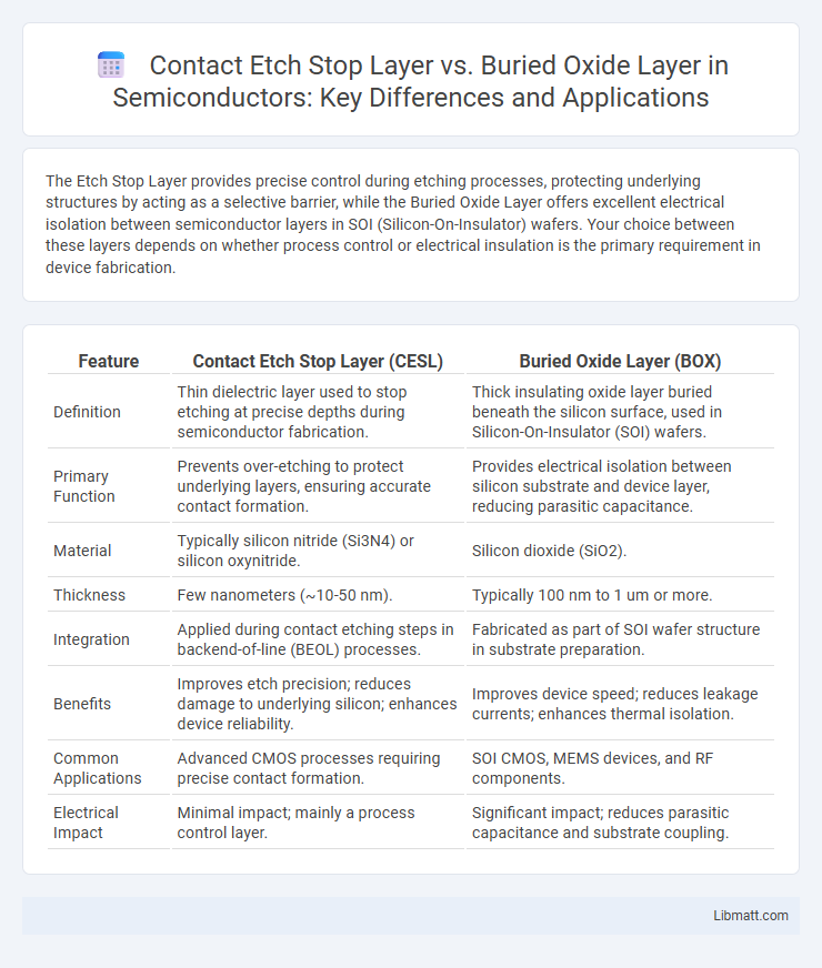
The Etch Stop Layer provides precise control during etching processes, protecting underlying structures by acting as a selective barrier, while the Buried Oxide Layer offers excellent electrical isolation between semiconductor layers in SOI (Silicon-On-Insulator) wafers. Your choice between these layers depends on whether process control or electrical insulation is the primary requirement in device fabrication.
Table of Comparison
| Feature | Contact Etch Stop Layer (CESL) | Buried Oxide Layer (BOX) |
|---|---|---|
| Definition | Thin dielectric layer used to stop etching at precise depths during semiconductor fabrication. | Thick insulating oxide layer buried beneath the silicon surface, used in Silicon-On-Insulator (SOI) wafers. |
| Primary Function | Prevents over-etching to protect underlying layers, ensuring accurate contact formation. | Provides electrical isolation between silicon substrate and device layer, reducing parasitic capacitance. |
| Material | Typically silicon nitride (Si3N4) or silicon oxynitride. | Silicon dioxide (SiO2). |
| Thickness | Few nanometers (~10-50 nm). | Typically 100 nm to 1 um or more. |
| Integration | Applied during contact etching steps in backend-of-line (BEOL) processes. | Fabricated as part of SOI wafer structure in substrate preparation. |
| Benefits | Improves etch precision; reduces damage to underlying silicon; enhances device reliability. | Improves device speed; reduces leakage currents; enhances thermal isolation. |
| Common Applications | Advanced CMOS processes requiring precise contact formation. | SOI CMOS, MEMS devices, and RF components. |
| Electrical Impact | Minimal impact; mainly a process control layer. | Significant impact; reduces parasitic capacitance and substrate coupling. |
Introduction to Contact Etch Stop Layer and Buried Oxide Layer
Contact Etch Stop Layer (CESL) is a thin dielectric film used in semiconductor devices to prevent damage to underlying layers during etching, ensuring precise patterning and improved device reliability. Buried Oxide Layer (BOX) is an insulating oxide layer situated beneath the silicon substrate in Silicon-On-Insulator (SOI) wafers, reducing parasitic capacitance and enhancing device performance. Understanding the distinct functions of CESL and BOX helps optimize your semiconductor fabrication processes for better electrical isolation and etch control.
Definitions: What is a Contact Etch Stop Layer?
A Contact Etch Stop Layer (CESL) is a thin dielectric film used in semiconductor fabrication to protect underlying layers during the etching process, ensuring precise pattern transfer and device integrity. It acts as a barrier, preventing etching chemicals from damaging sensitive regions beneath, thus enhancing layer selectivity and reducing defects. Your device's performance and yield benefit from the CESL's role in maintaining structural accuracy and minimizing process variability.
Understanding the Buried Oxide Layer (BOX)
The Buried Oxide Layer (BOX) in silicon-on-insulator (SOI) technology serves as a highly effective electrical insulator, reducing parasitic capacitance and enhancing device performance by isolating the active silicon layer from the substrate. This insulating layer, typically composed of silicon dioxide, enables improved thermal management and minimizes leakage current, critical for high-speed and low-power semiconductor devices. Proper understanding of the BOX layer's thickness and material properties is essential for optimizing device fabrication processes and ensuring reliable transistor operation.
Key Functions in Semiconductor Fabrication
The Contact Etch Stop Layer (CESL) acts as a protective barrier during etching processes, preventing damage to underlying layers and ensuring precise feature definition in semiconductor devices. The Buried Oxide Layer (BOX) primarily provides electrical isolation between the silicon substrate and the active device layers, reducing parasitic capacitance and improving device performance. Understanding these layers helps optimize Your semiconductor fabrication for enhanced device reliability and efficiency.
Material Composition and Properties
Contact Etch Stop Layer (CESL) typically consists of silicon nitride (Si3N4), valued for its high etch selectivity and excellent mechanical stress properties, which help protect underlying layers during etching processes. Buried Oxide Layer (BOX), commonly made of silicon dioxide (SiO2), provides electrical insulation and isolation in silicon-on-insulator (SOI) structures due to its low dielectric constant and excellent thermal stability. CESL enhances device performance by controlling strain and minimizing defects, while BOX ensures reduced parasitic capacitance and leakage, improving overall transistor reliability.
Process Integration: Placement in Device Structures
The Contact Etch Stop Layer (CESL) is typically integrated above the transistor's active channel to serve as an etch barrier during contact formation, ensuring precise patterning and minimizing damage to underlying layers. In contrast, the Buried Oxide (BOX) layer resides beneath the silicon device layer in SOI (Silicon-On-Insulator) structures, acting as an electrical insulator to reduce parasitic capacitance and enhance device isolation. Your device's performance benefits from strategic process integration of CESL for reliability and BOX for improved electrical insulation and reduced leakage currents.
Advantages of Contact Etch Stop Layer
The Contact Etch Stop Layer (CESL) offers precise etch selectivity, protecting underlying layers during semiconductor fabrication and enabling finer pattern control compared to Buried Oxide Layers (BOX). CESL enhances device performance by reducing parasitic capacitance and improving transistor isolation without the added thickness and thermal budget constraints typical of BOX layers. This results in more efficient scaling and compatibility with advanced CMOS processes, making CESL advantageous for high-density integrated circuits.
Benefits of Buried Oxide Layer
The Buried Oxide Layer (BOX) provides superior electrical insulation and reduces parasitic capacitance, leading to enhanced device performance and lower power consumption in semiconductor applications. It also offers excellent isolation between the substrate and active device layers, improving signal integrity and reliability. Your integrated circuits benefit from the BOX's thermal stability and resistance to leakage currents compared to the Contact Etch Stop Layer.
Comparative Analysis: Performance and Reliability
The Contact Etch Stop Layer (CESL) provides improved etch selectivity and reduced plasma damage during fabrication, enhancing transistor gate reliability and uniformity, while the Buried Oxide Layer (BOX) offers excellent electrical isolation and reduces parasitic capacitance in SOI devices, leading to higher device speed and lower leakage currents. CESL materials, typically silicon nitride, excel in mechanical stress modulation to boost channel mobility but may introduce stress-related reliability challenges, whereas BOX layers, made of high-quality silicon dioxide, deliver superior long-term device stability and thermal isolation essential for minimizing short-channel effects. Performance-wise, CESL enhances transistor drive current through stress engineering, while BOX structures improve overall circuit speed and power efficiency by isolating active regions; reliability is influenced by CESL's stress-induced traps versus BOX's robustness in suppressing substrate leakage and latch-up phenomena.
Applications and Future Trends in Microelectronics
The Contact Etch Stop Layer (CESL) is widely used in advanced CMOS technology to improve strain engineering and device performance, while the Buried Oxide Layer (BOX) is fundamental in Silicon-On-Insulator (SOI) wafers for reducing parasitic capacitance and leakage currents. CESL's applications extend to FinFET and nanowire transistors, enhancing carrier mobility by controlling stress, whereas BOX layers are critical in high-speed, low-power microelectronics, enabling better thermal isolation and device scaling. Future trends indicate CESL integration with emerging 3D architectures and novel channel materials, while BOX layers continue evolving through ultra-thin oxides and hybrid SOI technologies to support sub-3nm node devices and heterogeneous integration.
Contact Etch Stop Layer vs Buried Oxide Layer Infographic