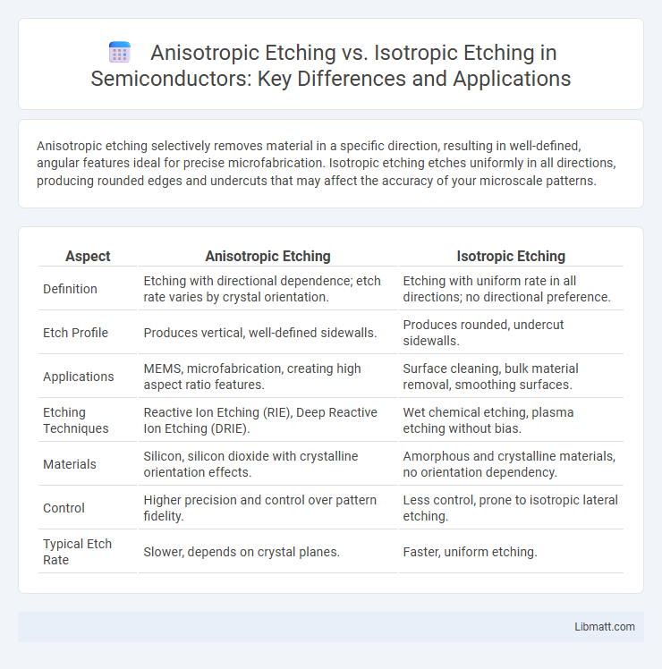
Anisotropic etching selectively removes material in a specific direction, resulting in well-defined, angular features ideal for precise microfabrication. Isotropic etching etches uniformly in all directions, producing rounded edges and undercuts that may affect the accuracy of your microscale patterns.
Table of Comparison
| Aspect | Anisotropic Etching | Isotropic Etching |
|---|---|---|
| Definition | Etching with directional dependence; etch rate varies by crystal orientation. | Etching with uniform rate in all directions; no directional preference. |
| Etch Profile | Produces vertical, well-defined sidewalls. | Produces rounded, undercut sidewalls. |
| Applications | MEMS, microfabrication, creating high aspect ratio features. | Surface cleaning, bulk material removal, smoothing surfaces. |
| Etching Techniques | Reactive Ion Etching (RIE), Deep Reactive Ion Etching (DRIE). | Wet chemical etching, plasma etching without bias. |
| Materials | Silicon, silicon dioxide with crystalline orientation effects. | Amorphous and crystalline materials, no orientation dependency. |
| Control | Higher precision and control over pattern fidelity. | Less control, prone to isotropic lateral etching. |
| Typical Etch Rate | Slower, depends on crystal planes. | Faster, uniform etching. |
Introduction to Etching Techniques
Etching techniques in semiconductor manufacturing include anisotropic etching, which removes material directionally to create precise, well-defined features, and isotropic etching, which etches uniformly in all directions, producing rounded or undercut profiles. Anisotropic etching is typically utilized in processes requiring high aspect ratio structures and sharp edges, often employing plasma or reactive ion etching methods. Isotropic etching is commonly applied in situations where uniform material removal is preferred, using wet chemical etchants like acids or bases to achieve smooth surface finishes.
Defining Anisotropic Etching
Anisotropic etching selectively removes material at different rates depending on the crystallographic orientation, producing well-defined, directional features in microfabrication processes. This technique contrasts isotropic etching, which etches uniformly in all directions, leading to rounded profiles. Understanding anisotropic etching allows you to achieve precise pattern transfer essential for semiconductor device fabrication and MEMS applications.
Defining Isotropic Etching
Isotropic etching removes material uniformly in all directions, producing rounded or undercut features instead of sharp profiles. Unlike anisotropic etching, which removes material directionally along specific crystallographic planes, isotropic etching etches both vertically and laterally at the same rate. Your choice between isotropic and anisotropic etching impacts the precision and geometry of microfabricated structures in semiconductor and MEMS devices.
Key Differences Between Anisotropic and Isotropic Etching
Anisotropic etching selectively removes material at different rates depending on the crystallographic orientation, resulting in highly directional and precise patterns ideal for MEMS and semiconductor fabrication. Isotropic etching, on the other hand, uniformly etches material in all directions, creating rounded or undercut features unsuitable for applications requiring sharp profiles. Understanding these key differences is crucial for optimizing your microfabrication processes and achieving the desired structural accuracy.
Advantages of Anisotropic Etching
Anisotropic etching offers precise control over the direction of material removal, leading to well-defined, vertical sidewalls critical for microfabrication and MEMS device manufacturing. This etching technique enables higher resolution pattern transfer compared to isotropic etching, which typically produces undercutting due to uniform etching in all directions. Your semiconductor or microelectronics projects benefit from improved dimensional accuracy and repeatability when using anisotropic etching processes.
Advantages of Isotropic Etching
Isotropic etching offers uniform material removal in all directions, enabling smooth and rounded feature profiles ideal for applications requiring gentle surface modifications. Its simplicity and cost-effectiveness make it suitable for large-scale production where precise directional control is less critical. You benefit from faster processing times and reduced complexity compared to anisotropic etching, which demands specialized equipment and conditions for directional etch control.
Applications in Semiconductor Fabrication
Anisotropic etching is favored in semiconductor fabrication for creating precise, well-defined structures such as microelectromechanical systems (MEMS) and integrated circuits due to its directional etching properties that produce sharp, vertical sidewalls. Isotropic etching, which etches uniformly in all directions, is typically used for applications requiring smooth, rounded features or when undercutting is necessary, such as in contact hole formation and surface cleaning. Your choice between anisotropic and isotropic etching techniques directly impacts device performance by influencing feature accuracy and surface morphology.
Material Compatibility and Process Selection
Anisotropic etching is highly compatible with crystalline materials like silicon, as it selectively etches along specific crystallographic planes, making it ideal for MEMS and semiconductor device fabrication where precision is crucial. Isotropic etching works well with a wider range of materials, including metals and polymers, by removing material uniformly in all directions, which is useful for applications requiring smooth, rounded profiles. When selecting your etching process, consider the material's crystallinity and desired feature geometry to achieve optimal etch profiles and device performance.
Challenges and Limitations
Anisotropic etching faces challenges in achieving uniform feature sizes due to variations in crystal orientation, which can lead to uneven etch rates and complex mask design requirements. Isotropic etching's primary limitation is its inability to produce precise, vertical sidewalls, resulting in undercutting that compromises the resolution and accuracy of microstructures. Your choice between these methods should consider the trade-offs between etched feature precision and process complexity based on specific application needs.
Future Trends in Etching Technology
Future trends in etching technology emphasize precise control of anisotropic etching to achieve high-aspect-ratio microstructures essential for advanced semiconductor devices. Innovations in plasma and reactive ion etching techniques are driving improvements in Selectivity and uniformity, enabling more complex and miniaturized components. Your ability to harness these cutting-edge etching processes will be critical for developing next-generation nanoscale fabrication technologies.
Anisotropic Etching vs Isotropic Etching Infographic