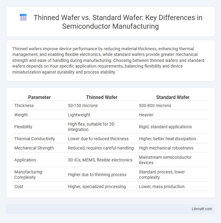
Thinned wafers improve device performance by reducing material thickness, enhancing thermal management, and enabling flexible electronics, while standard wafers provide greater mechanical strength and ease of handling during manufacturing. Choosing between thinned wafers and standard wafers depends on Your specific application requirements, balancing flexibility and device miniaturization against durability and process stability.
Table of Comparison
| Parameter | Thinned Wafer | Standard Wafer |
|---|---|---|
| Thickness | 50-150 microns | 500-800 microns |
| Weight | Lightweight | Heavier |
| Flexibility | High flex, suitable for 3D integration | Rigid, standard applications |
| Thermal Conductivity | Lower due to reduced thickness | Higher, better heat dissipation |
| Mechanical Strength | Reduced, requires careful handling | High mechanical robustness |
| Application | 3D ICs, MEMS, flexible electronics | Mainstream semiconductor devices |
| Manufacturing Complexity | Higher due to thinning process | Standard process, lower complexity |
| Cost | Higher, specialized processing | Lower, mass production |
Introduction to Semiconductor Wafers
Semiconductor wafers serve as the foundational substrates for integrated circuits, where standard wafers typically range from 200 to 300 micrometers in thickness, offering mechanical stability during processing. Thinned wafers, reduced to as thin as 50 micrometers or less, enable advanced applications such as flexible electronics and 3D stacking by improving heat dissipation and electrical performance. Your choice between thinned and standard wafers depends on device specifications, manufacturing constraints, and end-use functionality.
What is a Standard Wafer?
A standard wafer is a circular slice of semiconductor material, typically silicon, used as the substrate for microelectronic devices and integrated circuits. It usually measures between 100 mm and 300 mm in diameter, with a thickness optimized to balance mechanical strength and device fabrication requirements. Your choice of a standard wafer ensures compatibility with conventional manufacturing processes and equipment in semiconductor fabrication.
Understanding Thinned Wafers
Thinned wafers are semiconductor substrates that have been mechanically or chemically reduced in thickness from their original standard wafer size, improving flexibility and thermal performance in advanced electronic devices. These wafers allow for enhanced heat dissipation and enable the production of thinner, lighter, and more compact components in applications like flexible electronics and 3D integration. Understanding thinned wafers helps you optimize device performance and packaging in cutting-edge semiconductor manufacturing.
Manufacturing Processes Compared
Thinned wafers undergo a specialized backgrinding and polishing process to reduce their thickness, enhancing flexibility and enabling advanced packaging like 3D ICs or system-in-package assemblies. Standard wafers maintain a uniform thickness after slicing and chemical-mechanical polishing, optimizing mechanical stability for conventional semiconductor manufacturing. Your choice between thinned and standard wafers impacts device performance and packaging capabilities, as manufacturing processes are tailored to specific application requirements.
Physical & Mechanical Differences
Thinned wafers possess reduced thickness typically ranging from 50 to 200 microns, compared to standard wafers that generally measure around 725 microns, providing enhanced flexibility and improved thermal dissipation. Their decreased mass results in lower mechanical strength and increased fragility, making handling and processing more delicate relative to standard wafers. Understanding these physical and mechanical differences aids in selecting the appropriate wafer for applications requiring fine pitch interconnects or advanced packaging technologies, ensuring your semiconductor manufacturing process aligns with performance requirements.
Electrical Performance: Thinned vs Standard
Thinned wafers offer improved electrical performance due to reduced parasitic capacitance and shorter carrier transit times, resulting in faster signal propagation and lower power consumption compared to standard wafers. Your devices benefit from enhanced high-frequency operation and better thermal management, which is critical in advanced semiconductor applications. Standard wafers, while easier to handle, typically exhibit higher resistance and capacitance, limiting overall device speed and efficiency.
Applications of Thinned Wafers
Thinned wafers are extensively used in advanced semiconductor applications requiring reduced thickness for enhanced performance, such as in 3D integrated circuits, MEMS devices, and flexible electronics. Their reduced profile enables better thermal management and improved electrical characteristics critical for high-frequency and power devices. Standard wafers, while thicker and mechanically robust, are primarily suited for conventional planar device fabrication where structural integrity outweighs miniaturization.
Limitations and Challenges
Thinned wafers face significant limitations such as increased fragility and susceptibility to warping, complicating handling and processing during semiconductor manufacturing. These wafers require advanced equipment and techniques to prevent breakage and maintain structural integrity, leading to higher production costs compared to standard wafers. Additionally, challenges in thermal management arise due to reduced thickness, affecting heat dissipation and device performance in applications like high-power electronics.
Cost Implications and Scalability
Thinned wafers typically incur higher manufacturing costs due to additional processing steps like wafer thinning and handling precautions, impacting your overall budget in high-volume production. Standard wafers offer better scalability with established fabrication processes and supply chains, making them more cost-effective for large-scale semiconductor manufacturing. Choosing between thinned and standard wafers depends on balancing the precision and performance benefits against the increased expenses and production complexity.
Choosing the Right Wafer for Your Application
Selecting the right wafer depends on specific application requirements such as device flexibility, thermal management, and integration density. Thinned wafers offer reduced thickness for enhanced heat dissipation and better mechanical flexibility, making them ideal for advanced packaging and MEMS devices. Standard wafers provide greater structural robustness and ease of handling, suitable for high-volume production and conventional semiconductor fabrication.
Thinned Wafer vs Standard Wafer Infographic