A leadframe is a metal structure that provides mechanical support and electrical connections for semiconductor chips, while a substrate serves as the base layer onto which the semiconductor device is mounted, offering insulation and thermal management. Understanding the differences between leadframe and substrate materials can help optimize Your electronic packaging design for performance and reliability.
Table of Comparison
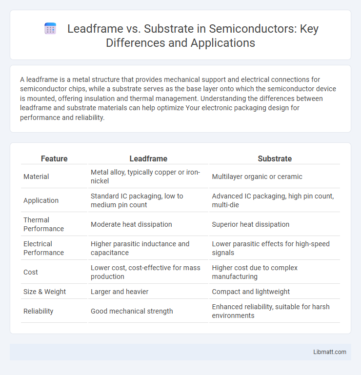
| Feature | Leadframe | Substrate |
|---|---|---|
| Material | Metal alloy, typically copper or iron-nickel | Multilayer organic or ceramic |
| Application | Standard IC packaging, low to medium pin count | Advanced IC packaging, high pin count, multi-die |
| Thermal Performance | Moderate heat dissipation | Superior heat dissipation |
| Electrical Performance | Higher parasitic inductance and capacitance | Lower parasitic effects for high-speed signals |
| Cost | Lower cost, cost-effective for mass production | Higher cost due to complex manufacturing |
| Size & Weight | Larger and heavier | Compact and lightweight |
| Reliability | Good mechanical strength | Enhanced reliability, suitable for harsh environments |
Introduction to Leadframe and Substrate
Leadframes are metal structures used as a mechanical support and electrical connection for semiconductor devices, typically made from copper or alloy materials and designed to fit within integrated circuit packages. Substrates serve as the base layer in semiconductor packaging, providing electrical pathways, mechanical support, and thermal dissipation, often composed of organic, ceramic, or glass materials. Both leadframes and substrates play critical roles in semiconductor device assembly, influencing performance, reliability, and package size.
Key Definitions and Terminology
Leadframe refers to a metal structure used in semiconductor packaging to provide mechanical support and electrical connection between the silicon chip and external circuitry. Substrate is a base material, often made of organic or ceramic compounds, that serves as a platform for mounting and interconnecting semiconductor devices. Understanding the distinction helps you optimize electronic component design by choosing appropriate materials for reliability and performance.
Material Composition: Leadframe vs Substrate
Leadframes are typically made from metal alloys such as copper, iron-nickel, or silver-palladium, offering excellent electrical conductivity and mechanical strength for semiconductor packaging. Substrates are composed of multilayered materials, including fiberglass-reinforced epoxy resin or ceramic, designed to provide insulation, thermal management, and structural support for electronic circuits. Your choice between leadframe and substrate hinges on the required balance of electrical performance, thermal dissipation, and mechanical reliability in your device.
Manufacturing Processes Compared
Leadframe manufacturing involves stamping or etching metal sheets to create precise conductive paths, providing a cost-effective and efficient solution for semiconductor packaging. Substrate production requires multilayer printed circuit boards with advanced materials, enabling higher complexity and enhanced electrical performance for sophisticated devices. Your choice depends on balancing manufacturing scalability, thermal management, and signal integrity needs.
Electrical Performance Differences
Leadframes offer lower electrical resistance and inductance due to their solid metal construction, enhancing signal integrity and power efficiency in high-frequency applications. Substrates, typically composed of organic or ceramic materials with embedded copper traces, provide better thermal management and support higher-density interconnections, impacting signal routing and impedance control. Your choice between leadframe and substrate will significantly influence the electrical performance based on frequency range, thermal requirements, and miniaturization goals.
Thermal Management Capabilities
Leadframe packaging offers moderate thermal conductivity due to its metal base, efficiently dissipating heat generated by semiconductor devices, which suits applications with standard power requirements. Substrate-based packaging provides superior thermal management through advanced materials like copper-invar-copper laminates, enhancing heat spread and supporting high-power, high-frequency components. Selecting between leadframe and substrate depends on the device's thermal dissipation needs, with substrates excelling in demanding thermal environments.
Cost Considerations and Scalability
Leadframes offer cost-effective manufacturing due to simpler stamping processes and lower material expenses, making them suitable for high-volume production. Substrates involve higher initial costs because of complex fabrication and multilayer designs but provide superior scalability for advanced electronic applications requiring miniaturization and higher interconnect density. Balancing cost considerations with scalability demands depends on the specific performance and volume requirements of semiconductor packaging projects.
Applications and Use Cases
Leadframes are widely used in semiconductor packaging, particularly for integrated circuits (ICs) in consumer electronics, automotive, and industrial applications, offering efficient electrical connectivity and thermal dissipation. Substrates find crucial applications in high-frequency and high-density semiconductor modules, such as RF devices, CPUs, and power modules, where advanced signal integrity and mechanical support are essential. Their use cases demonstrate that leadframes excel in cost-sensitive, high-volume production, while substrates are preferred for complex, high-performance electronic components requiring miniaturization and enhanced reliability.
Advantages and Disadvantages
Leadframe offers superior thermal conductivity and cost-effectiveness, making it ideal for high-volume packaging, but it may face limitations in miniaturization and electrical performance. Substrate provides better electrical insulation and supports higher input/output density, advantageous for advanced semiconductor packaging, though it tends to be more expensive and complex to manufacture. Your choice depends on balancing performance requirements with budget constraints and production scale.
Future Trends in Packaging Technologies
Leadframe and substrate technologies are evolving with the adoption of advanced materials like organic substrates and high-performance copper leadframes to enhance thermal management and electrical performance in semiconductor packaging. The integration of fan-out wafer-level packaging (FOWLP) and system-in-package (SiP) designs is driving demand for more flexible and miniaturized substrates, while leadframes continue to benefit from innovations in plating and molding techniques for improved reliability. Future trends emphasize heterogeneous integration and 3D packaging, where substrates and leadframes will play complementary roles in supporting higher input/output density and superior signal integrity.
Leadframe vs Substrate Infographic