BEOL (Back End of Line) refers to the process steps of fabricating the metal interconnections and insulating layers on a semiconductor wafer after transistor formation, while FEOL (Front End of Line) focuses on the initial stages of creating the transistor structures themselves within the silicon substrate. Understanding the differences between BEOL and FEOL is essential for optimizing semiconductor manufacturing and improving your chip's overall performance and reliability.
Table of Comparison
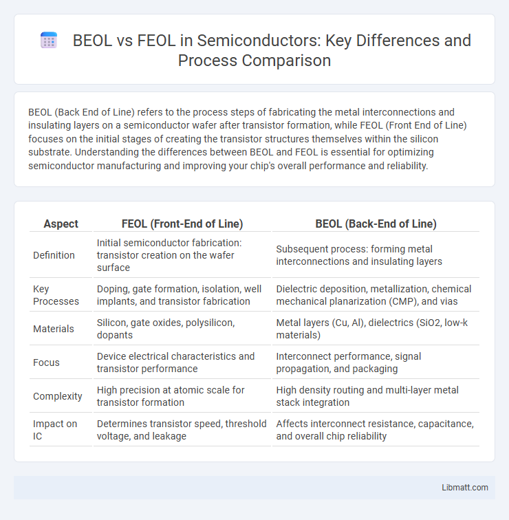
| Aspect | FEOL (Front-End of Line) | BEOL (Back-End of Line) |
|---|---|---|
| Definition | Initial semiconductor fabrication: transistor creation on the wafer surface | Subsequent process: forming metal interconnections and insulating layers |
| Key Processes | Doping, gate formation, isolation, well implants, and transistor fabrication | Dielectric deposition, metallization, chemical mechanical planarization (CMP), and vias |
| Materials | Silicon, gate oxides, polysilicon, dopants | Metal layers (Cu, Al), dielectrics (SiO2, low-k materials) |
| Focus | Device electrical characteristics and transistor performance | Interconnect performance, signal propagation, and packaging |
| Complexity | High precision at atomic scale for transistor formation | High density routing and multi-layer metal stack integration |
| Impact on IC | Determines transistor speed, threshold voltage, and leakage | Affects interconnect resistance, capacitance, and overall chip reliability |
Introduction to BEOL and FEOL
BEOL (Back-End-of-Line) and FEOL (Front-End-of-Line) represent distinct stages in semiconductor manufacturing, with FEOL involving the creation of transistor structures on the silicon wafer, while BEOL focuses on forming interconnects that connect these transistors. FEOL processes include doping, gate formation, and isolation, essential for defining device functionality, whereas BEOL encompasses metallization layers and dielectric deposition to enable electrical pathways. Understanding the differentiation between BEOL and FEOL is critical for optimizing your chip design and fabrication strategy.
Defining FEOL: Front-End Of Line
FEOL, or Front-End Of Line, refers to the initial phase in semiconductor manufacturing where the transistor structures are created on the silicon wafer, including processes like doping, gate formation, and well creation. This stage is crucial for defining the electrical characteristics and performance of the transistors, setting the foundation for subsequent steps. Understanding FEOL is essential for optimizing your chip design and ensuring device reliability.
Key Processes in FEOL Manufacturing
FEOL (Front-End-Of-Line) manufacturing involves critical key processes such as wafer preparation, oxidation, photolithography, ion implantation, and thin-film deposition to create transistor structures on the silicon wafer. These processes define the transistor's electrical characteristics by forming gate oxides, doped regions, and channel areas essential for device functionality. High precision in FEOL steps directly impacts semiconductor performance, device scaling, and yield before proceeding to BEOL interconnect formation.
Understanding BEOL: Back-End Of Line
Back-End Of Line (BEOL) refers to the crucial phase in semiconductor manufacturing where the metal interconnects are formed to link individual transistors and other components on the silicon wafer. This process includes depositing and patterning multiple layers of metal and dielectric materials to create the integrated circuit's wiring, enabling electrical communication between devices. Understanding BEOL is essential for optimizing signal integrity, performance, and reliability in advanced microchips.
BEOL Manufacturing Steps and Techniques
BEOL manufacturing involves processes such as dielectric deposition, photolithography, etching, and metal layer patterning to create interconnections on semiconductor wafers. Techniques like chemical vapor deposition (CVD) and physical vapor deposition (PVD) are commonly used to deposit insulating and conductive materials, while chemical-mechanical planarization (CMP) ensures surface uniformity for multi-layer stacking. Understanding these steps is crucial for optimizing your chip's performance and reliability in advanced semiconductor devices.
Major Differences Between BEOL and FEOL
Major differences between BEOL (Back-End-Of-Line) and FEOL (Front-End-Of-Line) lie in their processing stages and functions within semiconductor manufacturing. FEOL involves creating the transistor devices on the silicon wafer, including doping, gate formation, and isolation, which are critical for device performance and electrical characteristics. BEOL follows with the metallization processes, forming the interconnects through multiple metal layers and dielectric deposition to enable signal routing and power distribution in your integrated circuits.
Common Materials Used in FEOL vs BEOL
FEOL (Front-End-Of-Line) processes primarily utilize silicon, polysilicon, silicon dioxide (SiO2), and various dopants like boron and phosphorus to form transistors and other active devices. BEOL (Back-End-Of-Line) involves materials such as copper and aluminum for interconnects, low-k dielectrics for insulating layers, and tungsten for vias, optimizing signal transmission and electrical performance. Understanding the distinct materials in your semiconductor fabrication helps in improving device efficiency and scaling.
Technological Challenges in FEOL and BEOL
FEOL (Front-End-Of-Line) faces technological challenges such as scaling limitations of transistors, precise doping control, and complex lithography requirements for creating ultra-small device features. BEOL (Back-End-Of-Line) encounters challenges in interconnect scaling, managing parasitic capacitance and resistance, and integrating advanced materials for reliable metallization and low-k dielectrics. Both FEOL and BEOL demand innovations in fabrication techniques to meet the increasing performance and density requirements of modern semiconductor devices.
Impact on Semiconductor Device Performance
BEOL (Back-End-Of-Line) processes involve the formation of interconnects and metallization layers, significantly impacting signal integrity and power distribution, which directly influence semiconductor device performance. FEOL (Front-End-Of-Line) processes focus on transistor formation, such as gate oxide growth and doping concentration, determining the intrinsic electrical characteristics and switching speed of the device. Optimizing the integration between FEOL and BEOL layers is critical for minimizing parasitic capacitance and resistance, thereby enhancing overall circuit speed and energy efficiency.
Future Trends in BEOL and FEOL Technologies
Future trends in BEOL (Back-End-Of-Line) and FEOL (Front-End-Of-Line) technologies emphasize advanced materials and process innovations to enhance semiconductor performance and scalability. BEOL advancements focus on integrating low-k dielectrics and copper interconnects for reduced signal delay and power consumption, while FEOL progresses with extreme ultraviolet (EUV) lithography and novel transistor architectures like Gate-All-Around (GAA) to sustain Moore's Law. Your semiconductor designs will benefit from these trends, enabling higher density, improved speed, and energy efficiency in next-generation chips.
BEOL vs FEOL Infographic