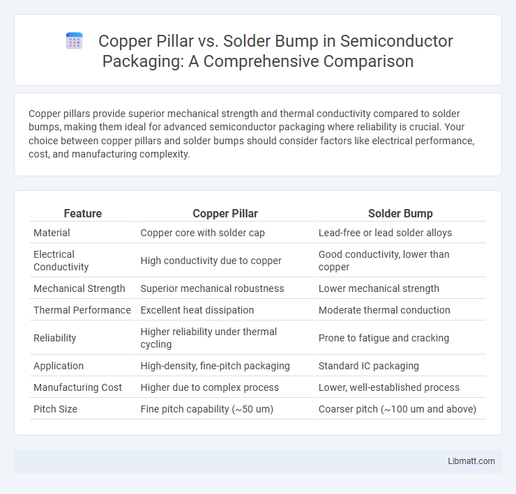
Copper pillars provide superior mechanical strength and thermal conductivity compared to solder bumps, making them ideal for advanced semiconductor packaging where reliability is crucial. Your choice between copper pillars and solder bumps should consider factors like electrical performance, cost, and manufacturing complexity.
Table of Comparison
| Feature | Copper Pillar | Solder Bump |
|---|---|---|
| Material | Copper core with solder cap | Lead-free or lead solder alloys |
| Electrical Conductivity | High conductivity due to copper | Good conductivity, lower than copper |
| Mechanical Strength | Superior mechanical robustness | Lower mechanical strength |
| Thermal Performance | Excellent heat dissipation | Moderate thermal conduction |
| Reliability | Higher reliability under thermal cycling | Prone to fatigue and cracking |
| Application | High-density, fine-pitch packaging | Standard IC packaging |
| Manufacturing Cost | Higher due to complex process | Lower, well-established process |
| Pitch Size | Fine pitch capability (~50 um) | Coarser pitch (~100 um and above) |
Introduction to Semiconductor Interconnects
Copper pillar and solder bump are critical semiconductor interconnect technologies enabling high-density, reliable connections in advanced packaging. Copper pillars offer superior mechanical strength, enhanced electrical conductivity, and better thermal dissipation compared to traditional solder bumps used in flip-chip assemblies. Your choice between these interconnects impacts device performance, assembly yield, and long-term reliability in semiconductor applications.
Overview of Copper Pillar Technology
Copper pillar technology features vertical copper columns with a solder cap used in advanced semiconductor packaging to enhance electrical performance and reliability. These copper pillars provide superior thermal conductivity and mechanical strength compared to traditional solder bumps, enabling finer pitch and higher input/output (I/O) density for integrated circuits. The technology supports improved signal integrity and reduced electromigration, making it essential for high-performance applications such as 3D IC packaging and system-in-package (SiP) solutions.
Understanding Solder Bump Technology
Solder bump technology involves creating small solder balls on semiconductor wafers to enable electrical and mechanical connections in flip-chip packaging, offering high-density interconnects and improved thermal performance. Copper pillar technology enhances this by incorporating a copper column with a solder cap, providing superior electrical conductivity, mechanical strength, and reliability under thermal stress compared to traditional solder bumps. Understanding solder bump technology is crucial for optimizing package design, ensuring robust interconnects, and advancing semiconductor device performance.
Key Differences Between Copper Pillar and Solder Bump
Copper Pillars offer higher mechanical strength and better electrical performance compared to Solder Bumps, making them ideal for fine-pitch applications and high-density interconnects. Solder Bumps rely on traditional tin-lead or lead-free solder, which can suffer from electromigration and thermal fatigue, whereas Copper Pillars provide enhanced reliability due to their robust copper core and thin solder cap. Your choice between these two depends on factors like assembly process, thermal management needs, and the desired lifespan of the electronic package.
Electrical Performance Comparison
Copper pillars offer superior electrical performance compared to solder bumps due to their lower electrical resistance and higher current-carrying capacity. The enhanced conductivity of copper pillars minimizes signal loss and improves overall signal integrity in high-frequency applications. Solder bumps, while cost-effective, exhibit higher resistance and are more prone to electromigration, which can degrade electrical reliability over time.
Thermal Conductivity and Heat Dissipation
Copper pillars exhibit significantly higher thermal conductivity, approximately 398 W/m*K, compared to solder bumps, which typically range around 50 W/m*K, enabling superior heat dissipation in electronic packages. This enhanced thermal performance reduces hotspots and improves the overall reliability and lifespan of integrated circuits by efficiently channeling heat away from active components. Consequently, copper pillars are preferred in high-power and high-frequency applications where effective thermal management is critical.
Reliability and Mechanical Strength
Copper pillars offer superior reliability and mechanical strength compared to solder bumps due to their higher hardness and better resistance to electromigration and thermal fatigue. Your device benefits from copper pillars' enhanced structural integrity, which reduces the risk of joint cracking under mechanical stress and thermal cycling. Solder bumps, while cost-effective, tend to exhibit lower fatigue life and are more prone to deformation and failure in harsh operating conditions.
Manufacturing Processes and Challenges
Copper pillar manufacturing involves electroplating copper onto a wafer to form bumps, requiring precise control of plating thickness and uniformity to avoid defects. Solder bump processes utilize solder alloys deposited through printing or electroplating, with challenges including controlling wetting behavior and preventing voids during reflow. Your choice between copper pillar and solder bump technologies impacts assembly yield and reliability due to these distinct manufacturing complexities.
Cost Analysis and Scalability
Copper pillars offer a cost advantage over solder bumps by reducing the need for underfill materials and enabling finer pitch interconnections, which lowers overall assembly expenses. The scalability of copper pillars supports higher input/output (I/O) density and improved electrical performance, making them suitable for advanced packaging in high-volume production. Solder bumps, while less costly initially, face challenges in scaling down to smaller pitches and maintaining reliability at high densities, increasing total cost in complex applications.
Applications and Future Trends in Advanced Packaging
Copper pillars offer superior electrical conductivity and mechanical strength compared to solder bumps, making them ideal for high-performance applications like 3D ICs and heterogeneous integration. Solder bumps remain popular for traditional flip-chip packaging due to established processes and cost-effectiveness. Your choice will depend on evolving industry demands for miniaturization, thermal management, and enhanced reliability, with copper pillars gaining traction in next-generation advanced packaging solutions.
Copper Pillar vs Solder Bump Infographic