A stepper uses a photomask to project circuit patterns onto a wafer in small sections with high precision, ideal for manufacturing semiconductors. A scanner moves the photomask and wafer simultaneously during exposure, enabling higher resolution and throughput, which benefits your microchip production efficiency.
Table of Comparison
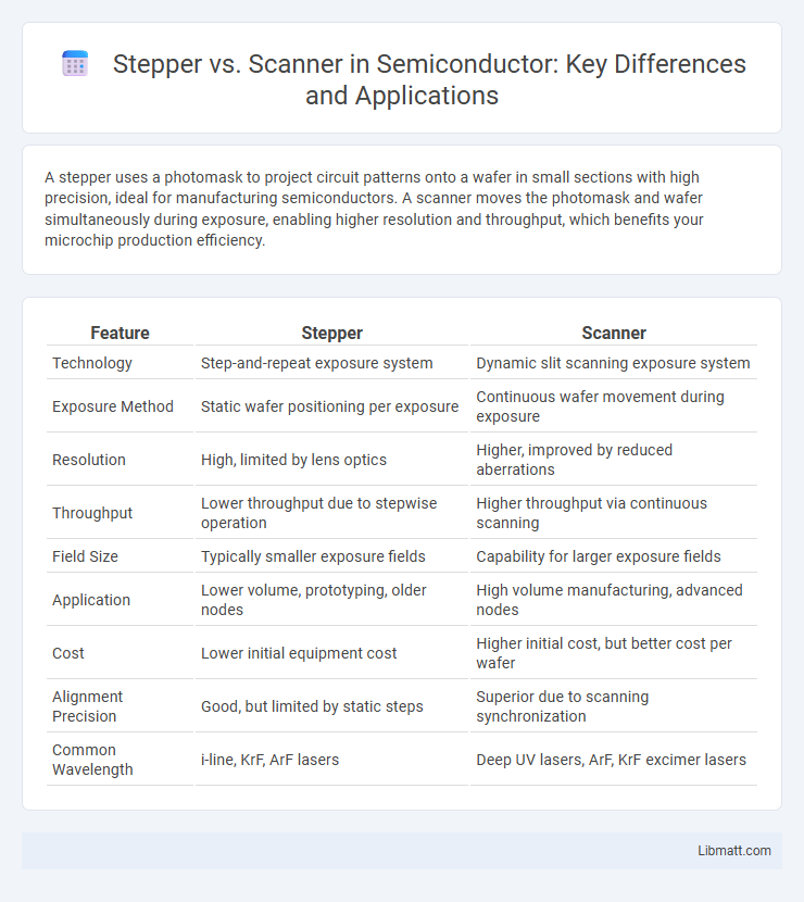
| Feature | Stepper | Scanner |
|---|---|---|
| Technology | Step-and-repeat exposure system | Dynamic slit scanning exposure system |
| Exposure Method | Static wafer positioning per exposure | Continuous wafer movement during exposure |
| Resolution | High, limited by lens optics | Higher, improved by reduced aberrations |
| Throughput | Lower throughput due to stepwise operation | Higher throughput via continuous scanning |
| Field Size | Typically smaller exposure fields | Capability for larger exposure fields |
| Application | Lower volume, prototyping, older nodes | High volume manufacturing, advanced nodes |
| Cost | Lower initial equipment cost | Higher initial cost, but better cost per wafer |
| Alignment Precision | Good, but limited by static steps | Superior due to scanning synchronization |
| Common Wavelength | i-line, KrF, ArF lasers | Deep UV lasers, ArF, KrF excimer lasers |
Introduction to Stepper and Scanner Technologies
Stepper and scanner technologies are critical in photolithography for semiconductor manufacturing, enabling precise pattern transfer onto silicon wafers. Steppers use a step-and-repeat method, projecting the mask pattern onto discrete wafer areas with high resolution, ideal for smaller production volumes and complex designs. Scanners employ a slit exposure with synchronized mask and wafer movement, achieving higher throughput and uniformity, making them suitable for mass production of advanced integrated circuits.
Key Differences Between Steppers and Scanners
Steppers use a fixed photomask and expose the wafer in successive, precise steps, offering superior resolution for advanced semiconductor manufacturing. Scanners move the photomask and wafer simultaneously during exposure, enabling higher throughput and improved overlay accuracy for large-scale production. The key differences lie in their exposure method, resolution capabilities, and suitability for different production volumes and technology nodes.
How Steppers Work: Principle and Applications
Steppers utilize a photolithography technique where a reticle projects an image of a microcircuit onto a wafer in successive, precise steps, enabling high-resolution patterning essential for semiconductor manufacturing. By advancing the wafer step-by-step under the lens, steppers achieve exceptional alignment accuracy, vital for creating intricate integrated circuits in CPUs and memory chips. Your choice of steppers influences fabrication throughput and device performance, making their principle and application critical in advanced microelectronics production.
How Scanners Operate: Principle and Applications
Scanners operate by emitting a focused beam of light that systematically moves across the surface of a subject, capturing detailed images through reflected light sensors. Utilizing principles such as laser triangulation or optical coherence tomography, scanners convert spatial information into precise digital data for analysis. These devices are widely applied in fields ranging from 3D modeling and medical imaging to quality control in manufacturing and document digitization.
Resolution and Precision: Stepper vs Scanner
Steppers provide precise and consistent resolution due to their mechanical grid movement, achieving sub-micron accuracy ideal for semiconductor lithography. Scanners excel in higher resolution capabilities through dynamic exposure and controlled light modulation, offering superior precision for complex patterning on advanced nodes. The choice between stepper and scanner hinges on the required resolution level and patterning intricacy, with scanners favored for ultra-fine features beyond the stepper's mechanical limits.
Throughput and Productivity Comparison
Steppers typically offer higher throughput for smaller production runs due to their flexibility in handling diverse wafer sizes and patterns, making them ideal for prototyping and low-volume manufacturing. Scanners, however, excel in productivity for high-volume production by delivering faster exposure speeds and better resolution through continuous wafer movement, reducing cycle times per wafer. Your choice between stepper and scanner should consider the trade-off between setup flexibility and throughput efficiency to maximize overall manufacturing productivity.
Cost Considerations: Initial and Long-Term
Stepper machines typically involve higher initial costs due to sophisticated optics and precision engineering, but offer lower long-term maintenance expenses and enhanced throughput efficiency. Scanners generally present a more affordable upfront investment, yet may incur increased operational costs over time due to faster wear and less accuracy, impacting yield. Your decision should weigh the balance between upfront capital expenditure and ongoing operational efficiency for optimal cost-effectiveness.
Suitability for Different Lithography Nodes
Steppers excel in lithography processes targeting advanced nodes like 7nm and below, offering superior resolution and alignment precision essential for cutting-edge semiconductor manufacturing. Scanners, suitable for larger nodes such as 28nm and above, deliver higher throughput by projecting the wafer through a moving reticle system, optimizing cost-efficiency for mature technology nodes. Your choice between steppers and scanners depends on the required resolution and volume demands inherent to the specific lithography node of your semiconductor fabrication.
Industry Trends and Future Prospects
The semiconductor manufacturing industry increasingly favors steppers over scanners due to their higher resolution capabilities and faster throughput, driving a shift in lithography technology adoption. Emerging trends highlight advancements in EUV (Extreme Ultraviolet) lithography, where steppers dominate owing to precise patterning essential for next-generation microchips. Future prospects indicate sustained investment in scanner technology for complex layers, but steppers will retain a leading role in high-volume, cost-effective chip production, reinforcing their strategic importance in the evolving semiconductor market.
Choosing the Right Solution: Stepper or Scanner?
Choosing the right solution between a stepper and a scanner depends on your specific lithography needs, including resolution requirements and throughput demands. Steppers offer higher resolution and precision for advanced semiconductor manufacturing, while scanners provide faster processing speeds suitable for high-volume production. Evaluating your process complexity and target device specifications will help determine whether a stepper or scanner aligns best with your manufacturing goals.
Stepper vs Scanner Infographic