Wafer dicing involves cutting semiconductor wafers into individual dies using a high-precision saw or laser, ensuring clean edges and minimal damage. Scribing creates shallow grooves on the wafer surface to facilitate easy breaking, offering a cost-effective alternative but with less precision and potential for chipping.
Table of Comparison
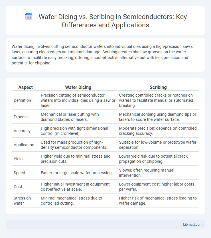
| Aspect | Wafer Dicing | Scribing |
|---|---|---|
| Definition | Precision cutting of semiconductor wafers into individual dies using a saw or laser. | Creating controlled cracks or notches on wafers to facilitate manual or automated breaking. |
| Process | Mechanical or laser cutting with diamond blades or lasers. | Mechanical scribing using diamond tips or lasers to score the wafer surface. |
| Accuracy | High precision with tight dimensional control (micron-level). | Moderate precision; depends on controlled cracking accuracy. |
| Application | Used for mass production of high-density semiconductor components. | Suitable for low-volume or prototype wafer separation. |
| Yield | Higher yield due to minimal stress and precision cuts. | Lower yield risk due to potential crack propagation or chipping. |
| Speed | Faster for large-scale wafer processing. | Slower, often requiring manual intervention. |
| Cost | Higher initial investment in equipment; cost-effective at scale. | Lower equipment cost; higher labor costs per wafer. |
| Stress on wafer | Minimal mechanical stress due to controlled cutting. | Higher risk of mechanical stress leading to wafer damage. |
Introduction to Wafer Dicing and Scribing
Wafer dicing and scribing are essential semiconductor manufacturing processes used to separate individual chips from a silicon wafer. Wafer dicing employs advanced saw blades or lasers to cut the wafer precisely along predefined streets, ensuring minimal damage to the die. Scribing uses a mechanical or laser scribe to create controlled cracks or grooves for easier breaking, offering a cost-effective option for certain wafer types and sizes.
Overview of Semiconductor Wafer Separation Techniques
Semiconductor wafer separation techniques include wafer dicing and scribing, both essential for dividing wafers into individual chips. Wafer dicing uses high-precision saw blades or lasers to cut through the silicon, ensuring clean and efficient separation with minimal damage. Your choice between dicing and scribing depends on factors such as wafer thickness, chip size, and production volume, impacting overall yield and device performance.
What is Wafer Dicing?
Wafer dicing is a precision process used to cut semiconductor wafers into individual microchips or dies by employing high-speed saws or lasers. This technique ensures the separation of functional semiconductor devices while maintaining the integrity of delicate circuits and minimizing mechanical stress. Wafer dicing is critical in semiconductor manufacturing due to its impact on yield, quality, and downstream assembly efficiency.
What is Wafer Scribing?
Wafer scribing involves creating precise, shallow trenches on a semiconductor wafer's surface to define individual die boundaries before separation. This technique uses a diamond-tipped tool or laser to weaken the wafer along specific lines without cutting all the way through, ensuring minimal stress and damage during die removal. Understanding wafer scribing allows you to optimize diced wafer quality and improve manufacturing yield in semiconductor device fabrication.
Key Differences Between Dicing and Scribing
Wafer dicing involves cutting semiconductor wafers into individual chips using high-precision saws or lasers, producing clean, separated dies. Scribing, on the other hand, creates shallow grooves or lines on the wafer surface by mechanical or laser scratching to facilitate later breaking or separation, with less precision and risk of cracking. Key differences center on the cutting depth, precision levels, and the resulting edge quality, with dicing ensuring fully separated dies and scribing acting as a preparatory step for mechanical snap separation.
Process Steps: Wafer Dicing vs. Scribing
Wafer dicing involves precise cutting of semiconductor wafers into individual dies using high-speed diamond blades or lasers, ensuring minimal damage and high throughput. Scribing, on the other hand, entails controlled scoring or scratching along predefined lines followed by mechanical breaking to separate the dies, typically used for less brittle materials or when cost efficiency is prioritized. Both processes require strict alignment and wafer handling techniques to maintain die integrity and yield quality in semiconductor manufacturing.
Pros and Cons of Wafer Dicing
Wafer dicing offers high precision and clean separation of semiconductor dies, making it ideal for complex microelectronic devices. However, it may result in higher costs due to specialized equipment and increased risk of die edge chipping compared to scribing methods. The technique also supports high throughput manufacturing but requires careful handling to minimize mechanical stress and ensure optimal die quality.
Pros and Cons of Wafer Scribing
Wafer scribing offers precise control over the wafer break lines, which reduces the risk of damaging adjacent chips and enables cleaner separation with minimal mechanical stress. However, scribing can be slower than dicing, and it may result in micro-cracks that impact wafer integrity if not properly controlled. Your choice should consider wafer material, chip size, and production volume to balance quality and throughput effectively.
Choosing the Right Method for Your Application
Wafer dicing offers high precision and is ideal for applications requiring minimal die damage and complex shapes, while scribing is cost-effective for simpler designs and less sensitive components. Selecting the right method depends on factors such as wafer material, die size, production volume, and final product requirements. Manufacturers must weigh the trade-offs between equipment cost, throughput, and edge quality to optimize yield and performance.
Future Trends in Wafer Separation Technologies
Emerging wafer separation technologies are shifting from traditional dicing methods toward advanced laser scribing and plasma dicing techniques, which offer higher precision and reduced micro-cracking risks. Innovations in robotic automation and AI-driven process control are enhancing throughput and yield in semiconductor manufacturing. Your choice of wafer separation method will increasingly rely on these future-proof technologies to meet the demands for smaller, more complex device geometries.
Wafer Dicing vs Scribing Infographic