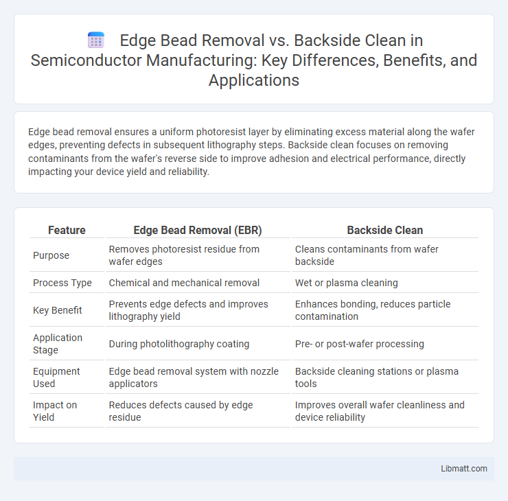
Edge bead removal ensures a uniform photoresist layer by eliminating excess material along the wafer edges, preventing defects in subsequent lithography steps. Backside clean focuses on removing contaminants from the wafer's reverse side to improve adhesion and electrical performance, directly impacting your device yield and reliability.
Table of Comparison
| Feature | Edge Bead Removal (EBR) | Backside Clean |
|---|---|---|
| Purpose | Removes photoresist residue from wafer edges | Cleans contaminants from wafer backside |
| Process Type | Chemical and mechanical removal | Wet or plasma cleaning |
| Key Benefit | Prevents edge defects and improves lithography yield | Enhances bonding, reduces particle contamination |
| Application Stage | During photolithography coating | Pre- or post-wafer processing |
| Equipment Used | Edge bead removal system with nozzle applicators | Backside cleaning stations or plasma tools |
| Impact on Yield | Reduces defects caused by edge residue | Improves overall wafer cleanliness and device reliability |
Introduction to Edge Bead Removal and Backside Clean
Edge Bead Removal (EBR) is a critical photolithography process that eliminates excess photoresist buildup along the wafer edges to prevent defects during subsequent manufacturing steps. Backside Clean targets contaminants, particles, and residues on the wafer's backside, ensuring optimal adhesion and preventing electrical shorts in advanced semiconductor devices. Both processes enhance yield and reliability by maintaining wafer surface integrity before packaging and assembly.
Importance of Cleanliness in Semiconductor Manufacturing
Edge Bead Removal (EBR) and Backside Clean are critical processes ensuring cleanliness in semiconductor manufacturing, preventing defects caused by contaminants on wafer surfaces. Effective edge bead removal minimizes resin buildup that can lead to poor adhesion or electrical faults, while backside cleaning eliminates particles and residues that might cause wafer handling issues or device yield loss. Maintaining pristine wafer surfaces through these methods enhances device reliability, improves process uniformity, and boosts overall semiconductor yield.
Edge Bead Removal: Process and Techniques
Edge Bead Removal (EBR) is a critical semiconductor fabrication process that eliminates excess photoresist from the wafer's edge to prevent defects during lithography and etching. Techniques such as spray solvent, edge bead etching, and laser ablation precisely remove the bead without compromising the wafer's active area. Your semiconductor manufacturing yield improves significantly by incorporating effective EBR methods that ensure uniform resist coverage and minimize particles on the wafer edge.
Backside Clean: Methods and Procedures
Backside clean techniques primarily involve plasma cleaning, chemical etching, and megasonic cleaning to remove contaminants and residues from the wafer's non-patterned side. Plasma cleaning utilizes reactive gases such as oxygen or argon to effectively eliminate organic films and particles, while chemical etching applies selective solvents or acids tailored to dissolve specific residues without damaging the wafer substrate. Megasonic cleaning employs high-frequency acoustic waves in ultrapure water to dislodge particulates, enhancing wafer surface quality and minimizing defects during subsequent lithography or deposition processes.
Key Differences Between Edge Bead Removal and Backside Clean
Edge Bead Removal (EBR) focuses on eliminating excess photoresist from the wafer's edge to prevent defects during semiconductor fabrication, while Backside Clean targets contaminants and residues on the wafer's backside to improve handling and adhesion in subsequent processes. EBR typically involves precise, localized techniques such as spray or vapor etching, whereas Backside Clean employs broader cleaning methods like chemical wipes or plasma treatments. Understanding these key differences helps optimize your wafer processing for higher yield and device reliability.
Impact on Yield and Device Performance
Edge Bead Removal enhances yield by preventing lithography defects caused by excess photoresist at wafer edges, leading to improved pattern fidelity and device uniformity. Backside Clean reduces particle contamination and wafer warpage, which directly improves device performance by minimizing electrical shorts and mechanical stress. Together, these processes are critical for maintaining high production yield and ensuring optimal semiconductor device functionality.
Challenges in Edge Bead Removal and Backside Clean
Edge bead removal (EBR) presents challenges such as inconsistent removal thickness and potential substrate damage due to chemical overexposure. Backside clean processes must address contamination from particles and residues without affecting front-side pattern integrity, requiring precise control of cleaning agents and techniques. Your semiconductor manufacturing yield depends heavily on effectively managing these challenges to avoid defects and ensure device reliability.
Equipment and Technologies Used
Edge bead removal utilizes specialized equipment such as programmable blade systems, ultrasonic bead removers, and plasma cleaning tools to precisely eliminate excess photoresist from wafer edges, enhancing lithography accuracy. In contrast, backside clean employs technologies like brush scrubbers, megasonic cleaners, and chemical etching systems designed to remove contaminants and residues from the wafer's non-patterned side, ensuring optimal device performance. Your choice between these processes depends on the specific equipment capabilities and technological requirements of your semiconductor fabrication workflow.
Industry Best Practices and Standards
Edge Bead Removal (EBR) and Backside Clean are critical processes in semiconductor manufacturing to ensure wafer uniformity and device reliability. Industry best practices emphasize precise control of EBR to prevent defects caused by photoresist accumulation at wafer edges, while Backside Clean standards focus on removing contaminants and particles to avoid device contamination and yield loss. Compliance with SEMI standards and implementation of automated inspection systems are essential to maintain high throughput and achieve superior process repeatability in both techniques.
Future Trends in Wafer Cleaning Processes
Future trends in wafer cleaning processes emphasize advancements in both Edge Bead Removal (EBR) and Backside Clean techniques to enhance yield and device reliability. Innovations focus on precision chemicals and optimized process control to minimize contamination and improve uniformity on wafer surfaces. You can expect increased automation and real-time monitoring systems to drive efficiency and reduce defect rates in semiconductor manufacturing.
Edge Bead Removal vs Backside Clean Infographic