Copper CMP offers superior planarization due to its softer nature and excellent conductivity, making it ideal for advanced semiconductor interconnects, while Tungsten CMP provides greater hardness and resistance, suitable for barrier and contact applications. Your choice depends on the specific requirements for surface uniformity, electrical performance, and integration complexity in microfabrication processes.
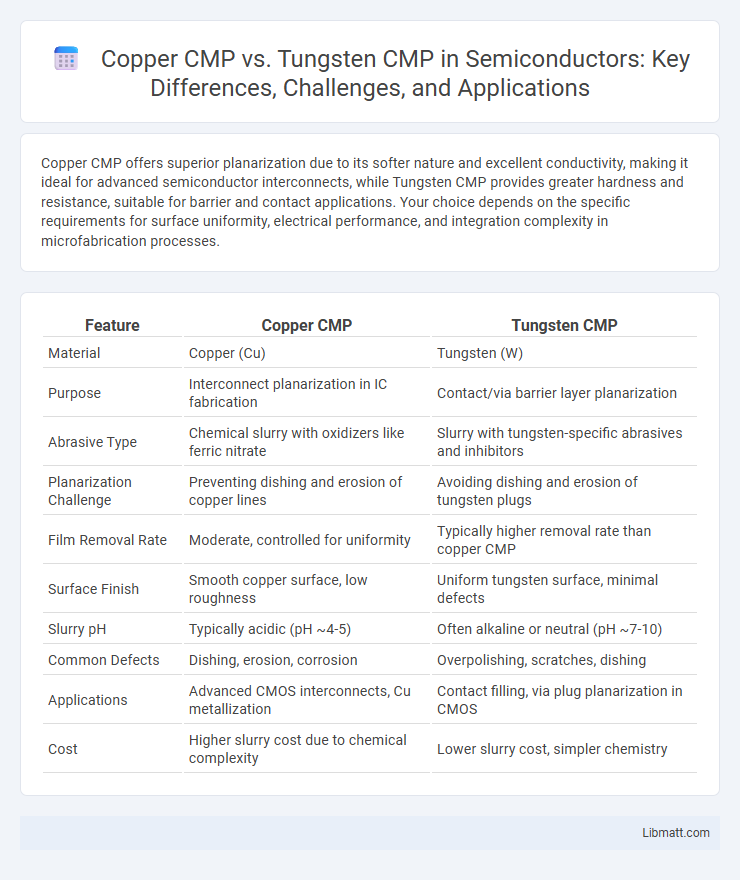
Table of Comparison
| Feature | Copper CMP | Tungsten CMP |
|---|---|---|
| Material | Copper (Cu) | Tungsten (W) |
| Purpose | Interconnect planarization in IC fabrication | Contact/via barrier layer planarization |
| Abrasive Type | Chemical slurry with oxidizers like ferric nitrate | Slurry with tungsten-specific abrasives and inhibitors |
| Planarization Challenge | Preventing dishing and erosion of copper lines | Avoiding dishing and erosion of tungsten plugs |
| Film Removal Rate | Moderate, controlled for uniformity | Typically higher removal rate than copper CMP |
| Surface Finish | Smooth copper surface, low roughness | Uniform tungsten surface, minimal defects |
| Slurry pH | Typically acidic (pH ~4-5) | Often alkaline or neutral (pH ~7-10) |
| Common Defects | Dishing, erosion, corrosion | Overpolishing, scratches, dishing |
| Applications | Advanced CMOS interconnects, Cu metallization | Contact filling, via plug planarization in CMOS |
| Cost | Higher slurry cost due to chemical complexity | Lower slurry cost, simpler chemistry |
Overview of CMP in Semiconductor Manufacturing
Chemical Mechanical Planarization (CMP) is a critical process in semiconductor manufacturing used to achieve ultra-flat surfaces necessary for subsequent photolithography steps. Copper CMP involves polishing copper interconnects, balancing selective removal rates between copper and the dielectric to prevent dishing and erosion, while Tungsten CMP is used for tungsten vias and contacts, focusing on minimizing dishing and maintaining integrity of the underlying barrier layers. Both processes require precise control of slurry chemistry, pad properties, and process parameters to ensure device performance and yield in advanced integrated circuits.
Introduction to Copper CMP
Copper CMP (Chemical Mechanical Planarization) is a critical process in semiconductor manufacturing that enables the planarization of copper interconnects, ensuring a smooth surface for subsequent photolithography steps. Copper CMP involves both chemical etching and mechanical polishing to remove excess copper while minimizing dishing and erosion, which are common challenges compared to Tungsten CMP. Its introduction marked a significant advancement over Tungsten CMP due to copper's superior electrical conductivity and reliability in advanced integrated circuits.
Introduction to Tungsten CMP
Tungsten CMP (Chemical Mechanical Planarization) is a critical process in semiconductor manufacturing used to achieve a smooth, planar surface by removing excess tungsten metal after deposition. Compared to copper CMP, tungsten CMP involves distinct slurry chemistries and polishing pads optimized to handle tungsten's hardness and chemical properties. Your choice between copper and tungsten CMP depends on the device architecture and material compatibility, with tungsten CMP excelling in applications requiring high hardness and excellent step coverage.
Key Differences Between Copper and Tungsten CMP
Copper CMP involves planarizing copper interconnects with slurries containing soft abrasives to achieve smooth, defect-free surfaces, while tungsten CMP uses harder abrasives designed to remove tungsten films and underlying barrier layers effectively. Copper CMP requires careful endpoint detection due to copper's tendency to over-polish and cause dishing, whereas tungsten CMP focuses on minimizing erosion and achieving uniform tungsten layer thickness. Process chemistries differ significantly, with copper CMP utilizing oxidation-reduction reactions and tungsten CMP relying on mechanical abrasion combined with selective chemical etching.
Process Chemistry: Copper vs. Tungsten CMP
Copper CMP relies on specialized slurry formulations containing oxidizers like hydrogen peroxide and complexing agents to form a copper oxide layer that is gently removed by a soft polishing pad, ensuring minimal dishing and erosion. Tungsten CMP utilizes abrasive slurries with oxidizers such as ferric nitrate to oxidize tungsten surfaces while employing harder polishing pads to effectively remove the tungsten oxide layer and underlying metal. The distinct chemical interactions and mechanical removal rates in Copper CMP versus Tungsten CMP directly impact planarization efficiency, defect control, and integration challenges in semiconductor fabrication.
Slurry Selection and Optimization
Slurry selection and optimization are critical in Copper CMP vs Tungsten CMP due to their distinct material properties; copper requires slurries with effective corrosion inhibitors and chelating agents to prevent dishing and erosion, while tungsten demands slurries with strong oxidizers and abrasive particles to achieve uniform tungsten removal without damaging the dielectric. Your process benefits from tailoring slurry pH, particle size, and chemistry to balance removal rates and surface planarity, enhancing overall CMP performance. Optimizing slurry composition for each metal ensures minimal defects, improved wafer yield, and consistent semiconductor device quality.
Challenges and Defect Management
Copper CMP faces challenges such as dishing and erosion due to its softer metal properties and complex barrier layer removal, requiring precise slurry chemistry and pad conditioning to minimize defects. Tungsten CMP encounters difficulties like dishing and residue removal from tungsten and oxide interfaces, demanding effective endpoint detection and tailored slurry formulations to control defects. Managing these process-specific issues ensures Your semiconductor device maintains structural integrity and electrical performance.
Cost Implications: Copper vs. Tungsten CMP
Copper CMP typically involves higher costs due to more complex slurry formulations and the necessity for robust polishing pads designed to handle copper's ductility. Tungsten CMP often proves more cost-effective because of simpler chemistries and lower consumable usage, but it may require additional barrier layer processing that can add to overall expenses. Your choice between copper and tungsten CMP will significantly impact fabrication costs depending on the specific integration and device requirements.
Applications in Advanced Node Technologies
Copper CMP excels in advanced node technologies due to its superior electrical conductivity and ability to form fine interconnects in sub-10nm semiconductor devices. Tungsten CMP is preferred for via filling and contact applications because of its excellent gap-filling properties and thermal stability in high aspect ratio structures. Your choice between Copper and Tungsten CMP processes depends on the specific interconnect requirements and device architecture in advanced semiconductor manufacturing.
Future Trends in CMP for Metallic Interconnects
Future trends in copper CMP emphasize improving dishing and erosion control through advanced slurry chemistries and endpoint detection technologies, addressing the need for ultra-flat surfaces in sub-5nm nodes. Tungsten CMP developments prioritize selectivity enhancements and defect reduction to maintain the integrity of barrier layers in 3D integration. Both materials see increased integration of machine learning for process optimization and real-time monitoring to boost throughput and yield in metallic interconnect fabrication.
Copper CMP vs Tungsten CMP Infographic