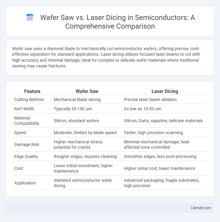
Wafer saw uses a diamond blade to mechanically cut semiconductor wafers, offering precise, cost-effective separation for standard applications. Laser dicing utilizes focused laser beams to cut with high accuracy and minimal damage, ideal for complex or delicate wafer materials where traditional sawing may cause fractures.
Table of Comparison
| Feature | Wafer Saw | Laser Dicing |
|---|---|---|
| Cutting Method | Mechanical blade slicing | Precise laser beam ablation |
| Kerf Width | Typically 50-150 um | As low as 10-30 um |
| Material Compatibility | Silicon, standard wafers | Silicon, GaAs, sapphire, delicate materials |
| Speed | Moderate; limited by blade speed | Faster; high precision scanning |
| Damage Risk | Higher mechanical stress, potential for cracks | Minimal mechanical damage, heat-affected zone controlled |
| Edge Quality | Rougher edges, requires cleaning | Smoother edges, less post-processing |
| Cost | Lower initial investment, higher maintenance | Higher initial cost, lower maintenance |
| Application | Standard semiconductor wafer dicing | Advanced packaging, fragile substrates, high precision |
Introduction to Wafer Singulation Techniques
Wafer singulation techniques primarily include wafer sawing and laser dicing, both essential for separating semiconductor dies with precision. Wafer saws use diamond-tipped blades to physically cut through silicon wafers, providing cost-effective and high-throughput singulation, particularly suited for standard silicon wafers. Laser dicing employs focused laser beams to ablate material, offering precise cuts with minimal mechanical stress, ideal for fragile or thin wafers used in advanced electronic applications.
Overview of Wafer Saw Technology
Wafer saw technology utilizes diamond-tipped blades to mechanically cut semiconductor wafers into individual dies with high precision and minimal damage. This method is widely favored for its cost-effectiveness and compatibility with various wafer materials and thicknesses. Your choice of wafer saw technology ensures precise die separation while maintaining structural integrity and minimizing contamination risks.
Fundamentals of Laser Dicing
Laser dicing uses focused laser beams to precisely cut semiconductor wafers, utilizing ultrafast pulses to minimize thermal damage and improve edge quality compared to traditional wafer saw methods. This technique offers higher precision and reduces mechanical stress, enhancing yield and reliability in microelectronic manufacturing. Your choice between wafer saw and laser dicing depends on factors like wafer thickness, material type, and required cut precision.
Key Differences Between Wafer Saw and Laser Dicing
Wafer saw and laser dicing are two prominent semiconductor wafer cutting techniques distinguished by their cutting methods; wafer saw uses a diamond blade to physically slice wafers, while laser dicing employs focused laser beams for precise, non-contact cutting. Wafer saw offers high throughput and is cost-effective for standard silicon wafers, but can introduce mechanical stress and cause chipping, whereas laser dicing excels in precision, minimal kerf loss, and suitability for thin, fragile, or hard materials without inducing mechanical damage. Your choice between these methods depends on factors like material type, device sensitivity, and production volume, with laser dicing preferred for advanced, delicate applications requiring superior edge quality.
Precision and Cut Quality Comparison
Wafer saw dicing delivers high mechanical precision with clean, straight cuts ideal for standard silicon wafers, but may cause micro-cracks near the edges. Laser dicing offers superior precision through non-contact ablation, enabling intricate patterns and minimal kerf width while reducing mechanical stress and chipping risks. The choice depends on the required cut quality, wafer thickness, and sensitivity to thermal effects during processing.
Impact on Yield and Throughput
Wafer saw dicing offers consistent high throughput for standard semiconductor wafers but can introduce mechanical stress leading to micro-cracks, which may reduce yield. Laser dicing provides precise, non-contact cutting that minimizes wafer damage and enhances yield, especially for thin or delicate wafers, but typically operates at lower throughput rates compared to mechanical sawing. Optimizing the choice between wafer saw and laser dicing depends on balancing the demand for high yield in sensitive applications with the production volume requirements.
Material Compatibility and Limitations
Wafer saw dicing is highly effective for silicon and other crystalline materials but struggles with brittle or thin substrates due to mechanical stress and chipping. Laser dicing offers versatility by precisely cutting a wide range of materials, including fragile, thin, and compound wafers, without physical contact or mechanical force. Limitations of laser dicing include thermal damage and slower throughput compared to traditional wafer saws, especially on thicker silicon wafers.
Cost Analysis: Wafer Saw vs Laser Dicing
Wafer saw dicing generally offers lower initial equipment costs and faster throughput for standard wafer sizes, making it cost-effective for high-volume production. Laser dicing incurs higher upfront investment but reduces material waste and enables finer precision, potentially lowering long-term expenses in advanced semiconductor applications. Operational costs vary significantly based on wafer thickness, device complexity, and yield requirements, influencing the overall cost-efficiency between wafer saw and laser dicing technologies.
Applications and Industry Adoption
Wafer Saw technology remains widely adopted in semiconductor manufacturing for applications requiring high precision and cost-efficiency in slicing silicon wafers into individual dies. Laser Dicing is increasingly favored in industries such as LED production and advanced microelectromechanical systems (MEMS) due to its ability to reduce mechanical stress and enable thinner, more complex wafer designs. Your choice depends on production volume, material sensitivity, and desired throughput, with wafer saws dominating traditional IC fabrication and laser dicing gaining momentum in cutting-edge applications.
Future Trends in Wafer Dicing Technologies
Wafer saw and laser dicing technologies are evolving rapidly to meet the demands of smaller, more complex semiconductors with increased precision and reduced kerf loss. Future trends in wafer dicing focus on hybrid methods combining mechanical sawing and laser techniques to optimize cutting speed and minimize micro-cracks, enhancing die strength and yield. Your choice of dicing technology will benefit from advancements like ultrafast lasers and AI-driven process control, which promise greater efficiency and adaptability in semiconductor manufacturing.
Wafer Saw vs Laser Dicing Infographic