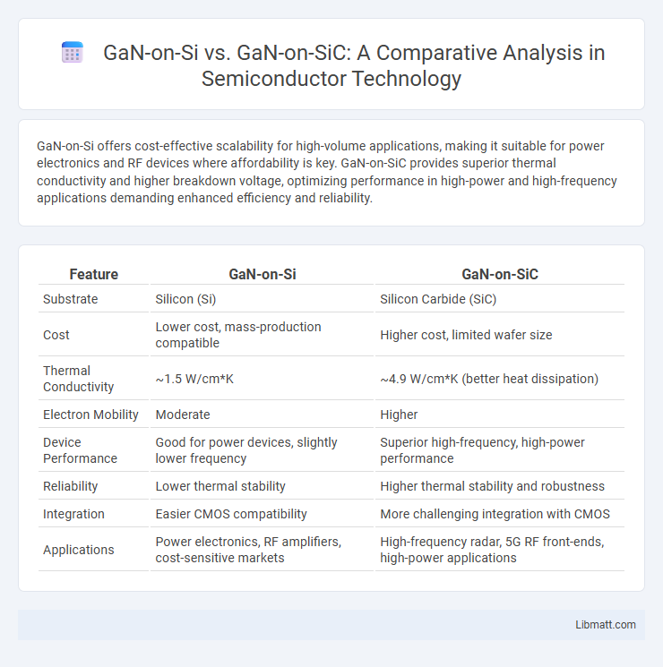
GaN-on-Si offers cost-effective scalability for high-volume applications, making it suitable for power electronics and RF devices where affordability is key. GaN-on-SiC provides superior thermal conductivity and higher breakdown voltage, optimizing performance in high-power and high-frequency applications demanding enhanced efficiency and reliability.
Table of Comparison
| Feature | GaN-on-Si | GaN-on-SiC |
|---|---|---|
| Substrate | Silicon (Si) | Silicon Carbide (SiC) |
| Cost | Lower cost, mass-production compatible | Higher cost, limited wafer size |
| Thermal Conductivity | ~1.5 W/cm*K | ~4.9 W/cm*K (better heat dissipation) |
| Electron Mobility | Moderate | Higher |
| Device Performance | Good for power devices, slightly lower frequency | Superior high-frequency, high-power performance |
| Reliability | Lower thermal stability | Higher thermal stability and robustness |
| Integration | Easier CMOS compatibility | More challenging integration with CMOS |
| Applications | Power electronics, RF amplifiers, cost-sensitive markets | High-frequency radar, 5G RF front-ends, high-power applications |
Introduction to GaN-on-Si and GaN-on-SiC Technologies
GaN-on-Si technology integrates gallium nitride layers on silicon substrates, offering cost-effective manufacturing and scalability for power electronics and RF applications. GaN-on-SiC combines gallium nitride with silicon carbide substrates, delivering superior thermal conductivity and higher electron mobility for enhanced performance in high-frequency and high-power devices. Both technologies leverage GaN's wide bandgap properties but differ fundamentally in substrate material characteristics influencing efficiency, thermal management, and device reliability.
Material Properties: Silicon vs Silicon Carbide Substrates
Gallium Nitride on Silicon Carbide (GaN-on-SiC) benefits from SiC's superior thermal conductivity of over 3.7 W/cm*K compared to silicon's 1.5 W/cm*K, enabling better heat dissipation and higher power density. Silicon substrates offer cost advantages and larger wafer sizes, but have lower thermal conductivity and higher lattice mismatch with GaN, which can impact device reliability. SiC substrates exhibit lower lattice mismatch and higher breakdown voltage, making GaN-on-SiC ideal for high-frequency, high-power applications requiring efficient thermal management.
Performance Comparison: Power Density and Efficiency
GaN-on-SiC substrates offer superior power density and efficiency compared to GaN-on-Si due to better thermal conductivity and lower on-resistance. GaN-on-Si devices typically exhibit higher cost and simplified manufacturing, but suffer from reduced breakdown voltage and efficiency under high power conditions. For high-power, high-frequency applications, GaN-on-SiC remains the preferred choice due to its robust thermal management and enhanced device performance.
Thermal Management and Heat Dissipation
GaN-on-SiC substrates exhibit superior thermal conductivity, typically around 370 W/m*K, enabling more efficient heat dissipation compared to GaN-on-Si substrates, which have thermal conductivity near 150 W/m*K. The enhanced thermal management of GaN-on-SiC reduces junction temperatures, improving device reliability and performance in high-power applications. GaN-on-Si substrates, while cost-effective, face challenges in heat spreading, requiring additional thermal management solutions to prevent overheating and maintain efficiency.
Cost Analysis: Fabrication and Scalability
GaN-on-Si offers significant cost advantages due to lower substrate expenses and compatibility with established silicon fabrication infrastructure, enabling scalable production for high-volume applications. In contrast, GaN-on-SiC exhibits superior thermal conductivity and device performance but incurs higher costs linked to expensive SiC substrates and more complex manufacturing processes. The scalability of GaN-on-Si is favored in commercial markets aiming for cost-effective, large-scale deployment despite GaN-on-SiC's premium performance benefits in niche, high-power environments.
Reliability and Device Lifetime
GaN-on-SiC devices demonstrate superior reliability and longer device lifetime compared to GaN-on-Si, due to SiC's excellent thermal conductivity and robust lattice compatibility, which reduce defect density and thermal stress during operation. GaN-on-Si devices often face challenges with lattice mismatch and silicon's lower thermal conductivity, leading to higher defect generation and accelerated degradation under high-power conditions. Your choice between GaN-on-Si and GaN-on-SiC will significantly impact device durability and performance stability in demanding applications.
RF and High-Frequency Applications
GaN-on-SiC substrates exhibit superior thermal conductivity and electron mobility compared to GaN-on-Si, making them ideal for high-frequency RF power amplifiers and radar systems. GaN-on-Si offers cost-effective scalability and integration with existing silicon processes but may face performance limitations in extreme high-frequency or high-power scenarios. Your choice depends on balancing performance needs with budget constraints for advanced RF and microwave applications.
Integration with Existing Semiconductor Processes
GaN-on-Si offers superior integration with existing semiconductor processes due to silicon's widespread use and mature fabrication infrastructure, enabling cost-effective production and easier scalability. GaN-on-SiC provides excellent high-power performance but faces challenges integrating with standard silicon-based manufacturing, limiting compatibility in mixed semiconductor environments. Your choice depends on balancing integration ease with performance requirements in advanced electronic applications.
Market Adoption and Industry Trends
GaN-on-Si technology is rapidly gaining market adoption due to its lower substrate cost and compatibility with existing silicon manufacturing infrastructure, making it attractive for high-volume power electronics applications. Conversely, GaN-on-SiC offers superior thermal conductivity and reliability, securing its position in high-performance sectors such as electric vehicles and aerospace, though at a higher cost. Industry trends indicate a growing hybrid approach, leveraging GaN-on-Si for consumer electronics and GaN-on-SiC for demanding environments, driving innovation and competitive pricing in both segments.
Future Developments and Research Directions
Future developments in GaN-on-Si technology focus on improving substrate quality and thermal management to enhance power density and reliability, making it a cost-effective alternative for high-frequency applications. GaN-on-SiC continues to gain ground with research targeting higher electron mobility and superior heat dissipation for extreme power and RF performance. Your choice between GaN-on-Si and GaN-on-SiC will depend on ongoing advancements in material integration and device scaling to meet evolving power electronics demands.
GaN-on-Si vs GaN-on-SiC Infographic