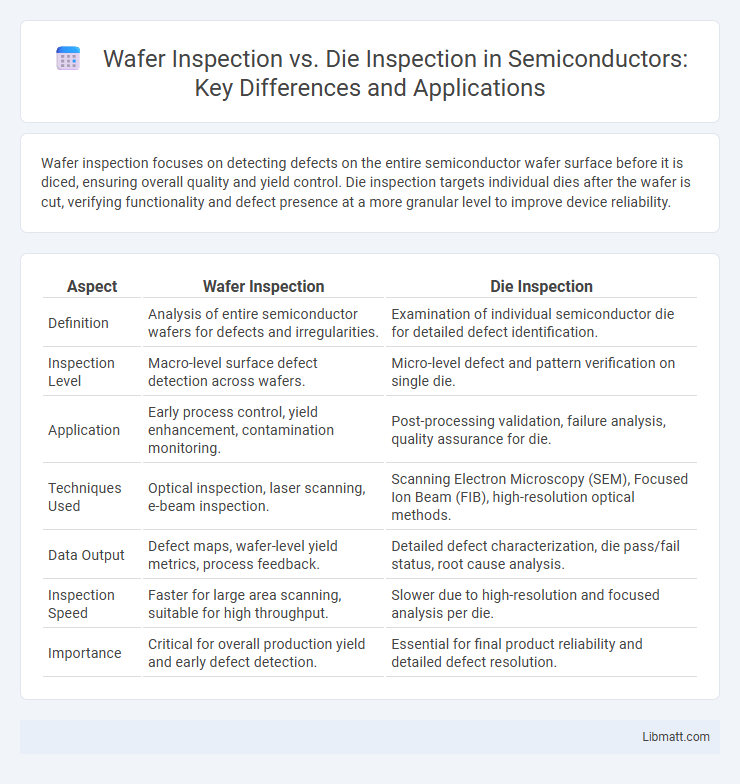
Wafer inspection focuses on detecting defects on the entire semiconductor wafer surface before it is diced, ensuring overall quality and yield control. Die inspection targets individual dies after the wafer is cut, verifying functionality and defect presence at a more granular level to improve device reliability.
Table of Comparison
| Aspect | Wafer Inspection | Die Inspection |
|---|---|---|
| Definition | Analysis of entire semiconductor wafers for defects and irregularities. | Examination of individual semiconductor die for detailed defect identification. |
| Inspection Level | Macro-level surface defect detection across wafers. | Micro-level defect and pattern verification on single die. |
| Application | Early process control, yield enhancement, contamination monitoring. | Post-processing validation, failure analysis, quality assurance for die. |
| Techniques Used | Optical inspection, laser scanning, e-beam inspection. | Scanning Electron Microscopy (SEM), Focused Ion Beam (FIB), high-resolution optical methods. |
| Data Output | Defect maps, wafer-level yield metrics, process feedback. | Detailed defect characterization, die pass/fail status, root cause analysis. |
| Inspection Speed | Faster for large area scanning, suitable for high throughput. | Slower due to high-resolution and focused analysis per die. |
| Importance | Critical for overall production yield and early defect detection. | Essential for final product reliability and detailed defect resolution. |
Introduction to Semiconductor Inspection
Wafer inspection and die inspection are critical processes in semiconductor manufacturing, ensuring the quality and functionality of microchips before packaging. Wafer inspection evaluates the entire silicon wafer for defects such as contamination, pattern deviations, and surface anomalies, while die inspection focuses on individual dies cut from the wafer, assessing electrical and structural integrity. Your semiconductor production's yield and reliability depend on precise defect detection at both wafer and die levels using advanced inspection technologies.
Understanding Wafer Inspection
Wafer inspection is a critical process in semiconductor manufacturing that detects surface defects and contamination on the entire wafer before dicing into individual dies. By identifying abnormalities such as particles, scratches, and pattern defects early, wafer inspection helps enhance yield and ensure the overall quality of semiconductor devices. Your manufacturing efficiency and final product reliability depend on precise wafer inspection techniques that complement, but differ from, the more detailed die inspection stage.
Defining Die Inspection
Die inspection involves the detailed examination of individual semiconductor dies after wafer dicing to identify defects that could affect device performance. Unlike wafer inspection, which scans the entire wafer for surface anomalies before dicing, die inspection targets each separated die to ensure functionality and yield. Your manufacturing process benefits from precise die inspection by enabling early detection of micro-level defects that impact chip reliability.
Key Differences Between Wafer and Die Inspection
Wafer inspection focuses on detecting defects, contaminations, and pattern deviations across the entire semiconductor wafer surface, ensuring uniformity before die separation. Die inspection targets individual dies post-wafer dicing, verifying critical functional and structural integrity to detect micro-level flaws affecting device performance. The key difference lies in the wafer inspection's broader scope for early defect identification, while die inspection provides detailed, die-specific quality assurance essential for final product reliability.
Inspection Techniques and Technologies
Wafer inspection primarily employs optical and electron microscopy techniques such as scanning electron microscopy (SEM) and laser scanning for defect detection on the wafer surface before dicing, emphasizing full-wafer mapping and pattern recognition algorithms. Die inspection uses more precise metrology tools including atomic force microscopy (AFM) and detailed 3D imaging systems to analyze individual die features after dicing, focusing on critical dimension measurement and anomaly detection at the die level. Both techniques integrate advanced machine learning models and automated defect classification systems to enhance accuracy and throughput in semiconductor manufacturing quality control.
Critical Defects Detected in Each Process
Wafer inspection primarily detects critical surface defects such as particles, scratches, and contamination that impact overall wafer yield. Die inspection focuses on identifying detailed functional defects including pattern irregularities, broken circuits, and electrical failures within individual dies. Combining both processes ensures comprehensive defect detection, optimizing semiconductor manufacturing quality control.
Impact on Yield and Production Quality
Wafer inspection targets defects on the entire wafer surface, enabling early detection of process variations that can significantly improve yield by preventing defective wafers from advancing through production. Die inspection focuses on individual dies after wafer dicing, identifying localized defects that affect final chip functionality and ensuring that only high-quality dies proceed to packaging and testing. Combining wafer and die inspections optimizes overall production quality by reducing defect-driven failures, minimizing scrap rates, and enhancing product reliability.
Challenges in Wafer vs Die Inspection
Wafer inspection faces challenges such as detecting defects on large, thin substrates prone to warping and particle contamination, complicating uniform illumination and precise defect localization across millions of dies. Die inspection requires higher resolution and sensitivity to identify micro-defects at the die level, demanding advanced imaging techniques to differentiate between process variations and actual defects. Both inspections must overcome throughput constraints while ensuring accuracy, but wafer inspection emphasizes scale and uniformity, whereas die inspection prioritizes defect granularity and classification fidelity.
Latest Innovations in Inspection Systems
Latest innovations in wafer inspection systems include advanced AI-powered defect detection algorithms and real-time imaging technologies that enhance throughput and accuracy. Die inspection has evolved with high-resolution optical sensors and machine learning models capable of identifying micro-level defects and pattern inconsistencies at speeds previously unattainable. Integration of multi-sensor data fusion and automated inline analysis further distinguishes modern inspection systems, enabling more precise quality control and yield optimization in semiconductor manufacturing.
Choosing the Right Inspection Strategy
Choosing the right inspection strategy involves understanding the distinct roles of wafer inspection and die inspection in semiconductor manufacturing. Wafer inspection targets surface defects and contamination across the entire wafer, enabling early detection of process issues, while die inspection focuses on identifying functional and structural defects within individual dies to ensure device performance. You should select wafer inspection for broad process control and die inspection for detailed quality assurance to optimize yield and reliability.
Wafer Inspection vs Die Inspection Infographic