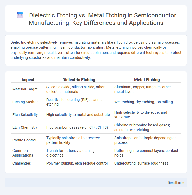
Dielectric etching selectively removes insulating materials like silicon dioxide using plasma processes, enabling precise patterning in semiconductor fabrication. Metal etching involves chemically or physically removing metal layers, often for circuit definition, and requires different techniques to protect underlying substrates and maintain conductivity.
Table of Comparison
| Aspect | Dielectric Etching | Metal Etching |
|---|---|---|
| Material Target | Silicon dioxide, silicon nitride, other dielectric materials | Aluminum, copper, tungsten, other metal layers |
| Etching Method | Reactive ion etching (RIE), plasma etching | Wet etching, dry etching, ion milling |
| Etch Selectivity | High selectivity to metal and substrate | High selectivity to dielectric and substrate |
| Etch Chemistry | Fluorocarbon gases (e.g., CF4, CHF3) | Chlorine or bromine-based gases; acids for wet etching |
| Profile Control | Typically anisotropic to preserve pattern fidelity | Anisotropic or isotropic depending on process |
| Common Applications | Trench formation, via etching in dielectrics | Patterning interconnect layers, contact holes |
| Challenges | Polymer buildup, etch residue control | Undercutting, surface roughness |
Introduction to Dielectric and Metal Etching
Dielectric etching involves the precise removal of insulating materials, such as silicon dioxide or silicon nitride, critical in semiconductor device fabrication to create patterns and trenches. Metal etching targets conductive layers like aluminum or copper, essential for defining circuit pathways and interconnects on integrated circuits. Understanding the distinct chemical and plasma processes used in both dielectric and metal etching is vital for optimizing your microfabrication workflow and achieving desired device performance.
Fundamental Principles of Etching Processes
Dielectric etching involves removing insulating materials such as silicon dioxide using reactive ion etching (RIE) with fluorocarbon gases, which selectively break down the dielectric layer while preserving underlying metals. Metal etching employs chemical or plasma-based methods that target metal films like aluminum or copper, using chlorine or bromine plasmas to achieve anisotropic etching with high precision. Both processes rely on controlling parameters like ion energy, gas chemistry, and chamber pressure to ensure selective material removal and maintain feature integrity in semiconductor fabrication.
Key Differences Between Dielectric and Metal Etching
Dielectric etching primarily targets insulating materials like silicon dioxide or silicon nitride, using plasma or reactive ion etching to create precise patterns without affecting conductive layers. Metal etching, on the other hand, involves removing metal layers such as aluminum or copper through wet chemical or dry etching processes, requiring careful control to prevent damage to underlying substrates. Understanding these key differences helps you select the appropriate etching method for specific semiconductor fabrication or microelectronic applications.
Common Materials Involved in Each Etching Type
Dielectric etching primarily involves materials such as silicon dioxide (SiO2), silicon nitride (Si3N4), and various oxides used as insulating layers in semiconductor devices. Metal etching commonly targets materials like aluminum, copper, tungsten, and titanium, which are frequently employed in interconnects and metallization layers of integrated circuits. Precise control of plasma chemistry and etching parameters is crucial for both etching types to achieve high selectivity and minimize damage to underlying layers.
Etching Mechanisms: Chemical vs Physical Processes
Dielectric etching primarily involves chemical reactions between reactive plasma species and the dielectric material, enabling selective removal through bond breaking and volatile byproduct formation. Metal etching often relies more on physical sputtering combined with chemical reactions, where energetic ions physically dislodge metal atoms while reactive species form volatile metal halides to enhance etch rates. These distinct mechanisms dictate process parameters such as gas chemistry, ion energy, and plasma density to optimize etch selectivity and profile control for dielectrics versus metals.
Equipment and Technologies Used
Dielectric etching primarily utilizes plasma etching equipment such as reactive ion etching (RIE) systems, which allow for precise anisotropic etching of insulating materials like silicon dioxide and silicon nitride. Metal etching often employs wet chemical etching with solutions like ferric chloride or electrochemical etching setups to selectively remove metal layers, such as aluminum or copper, used in semiconductor interconnects. Your choice between dielectric and metal etching depends on the compatibility of etching technologies with the material properties and the desired patterning resolution.
Applications in Semiconductor Manufacturing
Dielectric etching is primarily used in semiconductor manufacturing to create precise patterns and structures in insulating layers, such as silicon dioxide or silicon nitride, enabling isolation between conductive components on integrated circuits. Metal etching is essential for defining metallic interconnects and electrodes by selectively removing metal layers like aluminum or copper, facilitating electrical pathways and contacts. Both etching processes are critical for achieving device miniaturization, high performance, and yield in advanced semiconductor fabrication.
Process Challenges and Solutions
Dielectric etching faces challenges such as selectivity control, profile anisotropy, and microloading effects, often addressed by tuning plasma chemistry and employing advanced endpoint detection techniques. Metal etching struggles with issues like mask erosion, redeposition, and achieving high etch rates without damaging underlying layers, typically mitigated through optimized gas mixtures and temperature management. Both processes benefit from real-time process monitoring and adaptive control to enhance etch precision and minimize defects in semiconductor fabrication.
Etching Performance: Selectivity and Precision
Dielectric etching demonstrates superior selectivity by effectively targeting insulating layers like silicon dioxide while preserving underlying metal structures, leading to enhanced precision in microfabrication processes. Metal etching, optimized for conductive materials such as copper or aluminum, offers high anisotropy but generally presents lower selectivity, which can challenge the preservation of adjacent dielectric layers. Advanced plasma etching techniques improve control over etch rates and profiles in both dielectric and metal etching, enabling finer pattern resolution and reduced feature distortion.
Future Trends in Etching Technology
Future trends in etching technology emphasize increased precision and selectivity for both dielectric etching and metal etching processes, driven by the demand for smaller semiconductor nodes below 3nm. Advanced plasma etching techniques, including atomic layer etching (ALE), enable atomic-scale control, significantly improving feature resolution and minimizing damage to delicate materials. Integration of machine learning algorithms in etch process monitoring and control is expected to enhance yield and reduce variability in both dielectric and metal etching applications.
Dielectric Etching vs Metal Etching Infographic