ESD protection safeguards your electronic circuits from sudden electrostatic discharges by dissipating harmful voltage spikes, while latch-up protection prevents unintended high-current states caused by parasitic structures in integrated circuits, which can lead to device failure. Both mechanisms are crucial for enhancing the reliability and longevity of semiconductor devices in various applications.
Table of Comparison
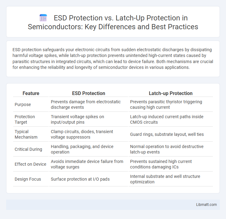
| Feature | ESD Protection | Latch-up Protection |
|---|---|---|
| Purpose | Prevents damage from electrostatic discharge events | Prevents parasitic thyristor triggering causing high current |
| Protection Target | Transient voltage spikes on input/output pins | Latch-up induced current paths inside CMOS circuits |
| Typical Mechanism | Clamp circuits, diodes, transient voltage suppressors | Guard rings, substrate layout, well ties |
| Critical During | Handling, packaging, and device operation | Normal operation to avoid destructive latch-up events |
| Effect on Device | Avoids immediate device failure from voltage surges | Prevents sustained high current conditions damaging ICs |
| Design Focus | Surface protection at I/O pads | Internal substrate and well structure optimization |
Introduction to ESD and Latch-up Phenomena
Electrostatic Discharge (ESD) occurs when a sudden flow of electricity passes between two electrically charged objects, potentially damaging semiconductor devices and integrated circuits. Latch-up is a parasitic, low-impedance path within CMOS circuits triggered by a voltage or current transient, causing high current flow and potential device malfunction or failure. Understanding ESD and latch-up phenomena is critical for designing effective protection mechanisms to enhance semiconductor reliability and prevent circuit damage.
What is ESD Protection?
ESD Protection safeguards electronic components from sudden electrostatic discharge events that can cause permanent damage to sensitive semiconductor devices. It involves integrating specialized materials and circuit elements like transient voltage suppressors and diode clamps to quickly divert and dissipate high-voltage spikes. This protection is critical for maintaining device reliability in environments prone to static electricity buildup and discharge.
What is Latch-up Protection?
Latch-up protection refers to design techniques implemented in integrated circuits to prevent the inadvertent triggering of a parasitic thyristor structure, which can cause a low-impedance path between power and ground lines, leading to device malfunction or destruction. This protection is critical in CMOS technology, where latch-up events can result in high current flow and permanent damage. Effective latch-up protection involves guard rings, substrate contacts, and layout optimization to enhance device reliability under electrical stress.
Key Differences Between ESD and Latch-up Events
ESD protection safeguards sensitive electronic components from sudden electrostatic discharges that cause immediate damage or data loss, while latch-up protection prevents a parasitic silicon-controlled rectifier within a semiconductor from triggering a short circuit that can lead to device failure. ESD events are transient and external, typically originating from human contact or environmental factors, whereas latch-up events are internal circuit malfunctions caused by voltage spikes or current surges. Your choice of protection strategy depends on whether you need to address external static discharge or internal device stability under electrical stress.
Common Causes of ESD and Latch-up
Electrostatic Discharge (ESD) commonly results from human contact, friction between materials, and charged device handling during manufacturing or operation, causing sudden high-voltage spikes that can damage semiconductor devices. Latch-up typically occurs due to parasitic structures within CMOS devices triggered by transient current injection, overvoltage, or ionizing radiation, leading to a low-impedance path and potential device failure. Your electronic circuits require both ESD and latch-up protection to guard against these distinct yet critical threats originating from different physical mechanisms and environmental interactions.
Techniques for ESD Protection in IC Design
Techniques for ESD protection in IC design include the integration of on-chip diodes, silicon-controlled rectifiers (SCRs), and MOS transistor-based clamps to divert and safely dissipate electrostatic discharge currents. These methods reduce the risk of device damage by controlling high-voltage spikes and improving circuit robustness. You can enhance your IC's reliability by carefully selecting and implementing these ESD mitigation structures without compromising performance.
Strategies for Effective Latch-up Protection
Effective latch-up protection strategies include implementing guard rings and well taps around sensitive regions in CMOS circuits to divert parasitic currents. Designing with silicon-on-insulator (SOI) technology and reducing the distance between p-n junctions minimize latch-up susceptibility. Careful layout techniques combined with diode clamps and proper substrate biasing enhance device robustness against latch-up events.
Impact of ESD and Latch-up on Semiconductor Reliability
Electrostatic discharge (ESD) causes sudden voltage spikes that can permanently damage semiconductor junctions, leading to reliability degradation and device failure. Latch-up, a parasitic thyristor action triggered by overvoltage or transient conditions, results in high current flow, potentially causing thermal runaway and permanent circuit damage. Implementing robust ESD and latch-up protection mechanisms is critical to maintaining semiconductor reliability and prolonging device lifespan in integrated circuits.
Industry Standards for ESD and Latch-up Immunity
Industry standards for ESD protection primarily include IEC 61000-4-2, JESD22-A114, and MIL-STD-883, which define testing methods and threshold levels for electrostatic discharge immunity in semiconductor devices. Latch-up immunity standards, such as JEDEC JESD78 and JEDEC JESD78A, focus on defining test procedures for evaluating a device's susceptibility to latch-up events caused by transient current spikes. Compliance with these standards ensures robust device performance and reliability in environments prone to electrostatic and transient electrical stresses.
Best Practices for Integrating ESD and Latch-up Protection
Integrating ESD and latch-up protection requires selecting components with optimized diode networks and robust transistor structures to withstand high-voltage transients and prevent parasitic triggering. You should place ESD protection devices close to input/output pads to minimize transient energy coupling, while latch-up protection often involves guard rings and well-tied substrates to isolate sensitive circuits. Combining these methods with careful PCB layout, including controlled impedance traces and proper grounding, ensures reliable semiconductor device performance under electrostatic and latch-up stress conditions.
ESD Protection vs Latch-up Protection Infographic