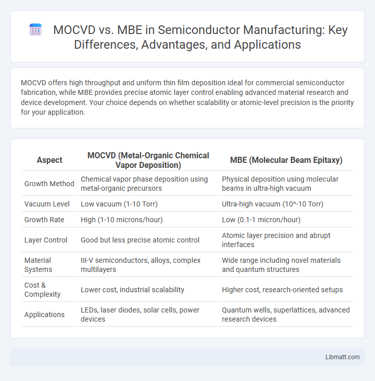
MOCVD offers high throughput and uniform thin film deposition ideal for commercial semiconductor fabrication, while MBE provides precise atomic layer control enabling advanced material research and device development. Your choice depends on whether scalability or atomic-level precision is the priority for your application.
Table of Comparison
| Aspect | MOCVD (Metal-Organic Chemical Vapor Deposition) | MBE (Molecular Beam Epitaxy) |
|---|---|---|
| Growth Method | Chemical vapor phase deposition using metal-organic precursors | Physical deposition using molecular beams in ultra-high vacuum |
| Vacuum Level | Low vacuum (1-10 Torr) | Ultra-high vacuum (10^-10 Torr) |
| Growth Rate | High (1-10 microns/hour) | Low (0.1-1 micron/hour) |
| Layer Control | Good but less precise atomic control | Atomic layer precision and abrupt interfaces |
| Material Systems | III-V semiconductors, alloys, complex multilayers | Wide range including novel materials and quantum structures |
| Cost & Complexity | Lower cost, industrial scalability | Higher cost, research-oriented setups |
| Applications | LEDs, laser diodes, solar cells, power devices | Quantum wells, superlattices, advanced research devices |
Introduction to Epitaxial Growth Techniques
Metalorganic Chemical Vapor Deposition (MOCVD) and Molecular Beam Epitaxy (MBE) are advanced epitaxial growth techniques used to deposit crystalline layers with high precision. MOCVD utilizes chemical vapor precursors to form thin films through surface reactions at elevated temperatures, offering high throughput for compound semiconductor fabrication. In contrast, MBE relies on atomic or molecular beams under ultra-high vacuum, enabling atomic-layer control and superior interface quality critical for quantum device applications.
Overview of MOCVD (Metal-Organic Chemical Vapor Deposition)
Metal-Organic Chemical Vapor Deposition (MOCVD) is a versatile thin-film deposition technique widely used in semiconductor manufacturing for producing high-quality epitaxial layers. Utilizing metal-organic precursors and hydrides, MOCVD enables precise control over film composition, thickness, and doping, making it ideal for fabricating LEDs, laser diodes, and high-electron-mobility transistors. The process operates at relatively high pressures and temperatures, benefiting from scalable wafer coverage and uniformity compared to Molecular Beam Epitaxy (MBE), which is favored for ultra-high vacuum growth of atomically precise layers.
Overview of MBE (Molecular Beam Epitaxy)
Molecular Beam Epitaxy (MBE) is a highly controlled process used to grow ultra-thin crystalline layers with atomic precision, essential for semiconductor device fabrication. Unlike MOCVD, MBE operates under ultra-high vacuum, allowing for precise control over layer composition and thickness, making it ideal for research and complex heterostructures. Your ability to tailor material properties at the atomic level makes MBE indispensable in developing advanced electronic and optoelectronic devices.
Process Mechanisms: MOCVD vs MBE
Metal-Organic Chemical Vapor Deposition (MOCVD) utilizes chemical reactions of metal-organic precursors on a heated substrate to deposit thin films, enabling high growth rates and excellent uniformity over large areas. Molecular Beam Epitaxy (MBE) relies on the physical evaporation of elemental sources in an ultra-high vacuum, allowing atomic-level control and precise layering with lower growth rates. MOCVD's process involves complex gas-phase and surface chemistry, whereas MBE depends on direct atomic beam fluxes and surface adsorption-desorption dynamics.
Material Quality and Purity Comparison
MOCVD (Metal-Organic Chemical Vapor Deposition) generally offers superior uniformity and smoothness in epitaxial layers, making it ideal for large-scale production with consistent material quality. In contrast, MBE (Molecular Beam Epitaxy) provides unparalleled control at the atomic level, resulting in extremely high purity and defect-free materials crucial for research and specialized device fabrication. Your choice will depend on whether prioritizing large-area uniformity or atomic-level precision is more critical for your application.
Growth Rate and Throughput Analysis
Metalorganic Chemical Vapor Deposition (MOCVD) offers significantly higher growth rates compared to Molecular Beam Epitaxy (MBE), with typical deposition speeds ranging from 1 to 10 microns per hour, enabling greater throughput for industrial-scale applications. MBE growth rates are much slower, generally on the order of a few monolayers per second, which limits throughput but allows for superior atomic-level control and precision. Your choice between MOCVD and MBE will depend on whether speed and volume or ultra-high precision are the priority for your semiconductor manufacturing process.
Equipment Complexity and Operational Costs
MOCVD systems typically feature more complex equipment with multiple gas delivery lines and intricate temperature controls, leading to higher initial investment costs compared to MBE. MBE setups rely on ultra-high vacuum chambers and effusion cells, resulting in relatively lower operational expenses but require precise maintenance to avoid contamination. Your choice between MOCVD and MBE will significantly influence both equipment complexity and long-term operational costs based on the specific application requirements.
Applications: MOCVD vs MBE in Industry
MOCVD excels in producing high-volume, uniform semiconductor devices such as LEDs, laser diodes, and power electronics, making it the preferred choice in commercial manufacturing due to its scalability and cost-efficiency. MBE offers superior precision in epitaxial layer growth, ideal for research and development of advanced quantum devices, high-electron-mobility transistors (HEMTs), and ultra-thin heterostructures used in niche applications requiring atomic-level control. Your selection between MOCVD and MBE will depend on whether industrial-scale production or experimental material properties are the primary focus.
Recent Advancements and Innovations
Recent advancements in Metal-Organic Chemical Vapor Deposition (MOCVD) emphasize enhanced precursor delivery systems and real-time in-situ monitoring, enabling superior control over film uniformity and composition at the atomic level. Molecular Beam Epitaxy (MBE) innovations concentrate on ultra-high vacuum improvements and atomic layer precision, facilitating complex heterostructure fabrication with minimal defects. Both methods now integrate machine learning algorithms to optimize growth parameters, significantly advancing semiconductor device performance and reliability.
Choosing the Right Technique for Your Needs
MOCVD offers high throughput and uniform deposition suitable for large-scale semiconductor manufacturing, while MBE provides atomic-level precision ideal for research and specialized device fabrication. Your choice depends on factors like desired film quality, layer complexity, and production volume. Evaluating these parameters ensures selecting the technique that aligns best with your specific application requirements.
MOCVD vs MBE Infographic