EPI doping offers precise control of dopant concentration and placement at the atomic layer, enhancing device performance compared to bulk doping methods that introduce dopants throughout the entire material volume. Your semiconductor fabrication benefits from epitaxial doping by achieving higher electrical uniformity and minimizing defects often associated with bulk doping techniques.
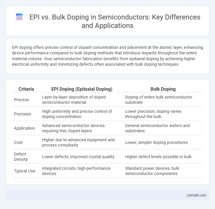
Table of Comparison
| Criteria | EPI Doping (Epitaxial Doping) | Bulk Doping |
|---|---|---|
| Process | Layer-by-layer deposition of doped semiconductor material | Doping of entire bulk semiconductor substrate |
| Precision | High uniformity and precise control of doping concentration | Lower precision; doping varies throughout the bulk |
| Application | Advanced semiconductor devices requiring thin, doped layers | General semiconductor wafers and substrates |
| Cost | Higher due to advanced equipment and process complexity | Lower, simpler doping procedures |
| Defect Density | Lower defects, improved crystal quality | Higher defect levels possible in bulk |
| Typical Use | Integrated circuits, high-performance devices | Standard power devices, bulk semiconductor components |
Introduction to EPI and Bulk Doping
Epitaxial (EPI) doping involves growing a single crystal layer on a semiconductor substrate with precise control over dopant concentration, resulting in uniform electrical properties ideal for high-performance devices. Bulk doping introduces dopants directly into the entire semiconductor wafer during crystal growth, affecting the entire volume and typically used for large-scale, cost-effective production. Your choice between EPI and bulk doping impacts device performance, scalability, and fabrication complexity.
Definition and Process of EPI Doping
Epitaxial (EPI) doping involves adding impurities to a thin, single-crystal silicon layer grown atop a substrate, allowing precise control over dopant concentration and distribution. This process uses chemical vapor deposition to grow the epitaxial layer while introducing dopant gases, resulting in a highly uniform and controlled doping profile. Unlike bulk doping, which modifies the entire wafer, EPI doping targets only the epitaxial layer, enhancing device performance by minimizing defects and optimizing electrical characteristics.
Explanation of Bulk Doping Techniques
Bulk doping techniques involve introducing dopants directly into the semiconductor substrate during crystal growth, enabling uniform distribution of impurities throughout the material. Common methods include diffusion, where dopants are introduced at high temperatures to penetrate the substrate, and ion implantation, which uses accelerated ions to embed dopants precisely at desired depths. These techniques control electrical properties by adjusting dopant concentration and depth, crucial for device performance in integrated circuits and power electronics.
Material Compatibility in EPI vs Bulk Doping
Epitaxial (EPI) doping offers superior material compatibility compared to bulk doping by allowing precise control over dopant profiles within a single crystalline layer, minimizing lattice defects and strain. Bulk doping often introduces higher concentrations of impurities throughout the substrate, which can lead to increased dislocations and degrade semiconductor device performance. EPI techniques utilize atomic-level deposition processes that maintain the substrate's crystal structure integrity, enhancing the overall material quality for advanced semiconductor applications.
Precision and Control in Doping Levels
EPI (Epitaxial) doping offers superior precision and control over doping levels compared to bulk doping by enabling atomic-scale layer-by-layer incorporation of dopants during semiconductor crystal growth. This method allows for tailored electrical properties and minimizes defects, ensuring consistent device performance. Your semiconductor manufacturing process benefits from EPI doping's ability to achieve highly uniform and reproducible dopant concentrations.
Advantages of EPI Doping
EPI doping offers superior control over dopant distribution, enabling precise and uniform incorporation of impurities at the atomic scale, which enhances device performance. This method significantly reduces defects and contamination compared to bulk doping, resulting in higher-quality epitaxial layers with improved electrical characteristics. Your semiconductor devices benefit from faster switching speeds and increased reliability due to the optimized junction profiles achievable through EPI doping.
Benefits of Bulk Doping
Bulk doping offers enhanced uniformity in dopant distribution throughout the semiconductor material, resulting in improved electrical characteristics and device reliability. This method enables precise control over dopant concentration, which optimizes carrier mobility and reduces defects compared to selective techniques like EPI. Your semiconductor devices benefit from increased performance stability and consistent fabrication outcomes using bulk doping methods.
Limitations and Challenges of Each Method
Epitaxial (EPI) doping faces limitations such as high processing costs, stringent temperature control requirements, and potential contamination affecting layer uniformity. Bulk doping encounters challenges like limited precision in dopant distribution, reduced control over junction depths, and difficulties in achieving ultra-shallow profiles critical for advanced semiconductor devices. Both methods struggle with balancing dopant concentration and electrical characteristics while maintaining material integrity during fabrication.
Applications in Semiconductor Device Fabrication
Epitaxial (EPI) doping enables precise control of dopant concentration and distribution, critical for advanced semiconductor devices like high-speed transistors and integrated circuits. Bulk doping introduces dopants uniformly throughout the substrate, suitable for simpler devices such as power electronics and basic diodes. EPI doping offers superior electrical properties and reduced defects, enhancing device performance in nanoscale fabrication processes.
Future Trends: EPI vs Bulk Doping Technologies
Future trends in semiconductor manufacturing show a growing preference for EPI doping due to its superior control over dopant concentration and uniformity, essential for advanced device performance. Bulk doping remains relevant for cost-effective production of standard components but faces limitations in scaling for next-generation miniaturized circuits. Your choice between EPI and bulk doping will hinge on balancing precision requirements against production efficiency as device architectures evolve.
EPI vs Bulk Doping Infographic