OFC (Optical Field Confinement) lithography offers enhanced resolution for advanced semiconductor manufacturing by tightly controlling light exposure patterns, while DUV (Deep Ultraviolet) lithography uses shorter wavelengths to achieve fine feature sizes on chips. Your choice between OFC and DUV lithography depends on factors like required pattern precision, wavelength capabilities, and production cost efficiency.
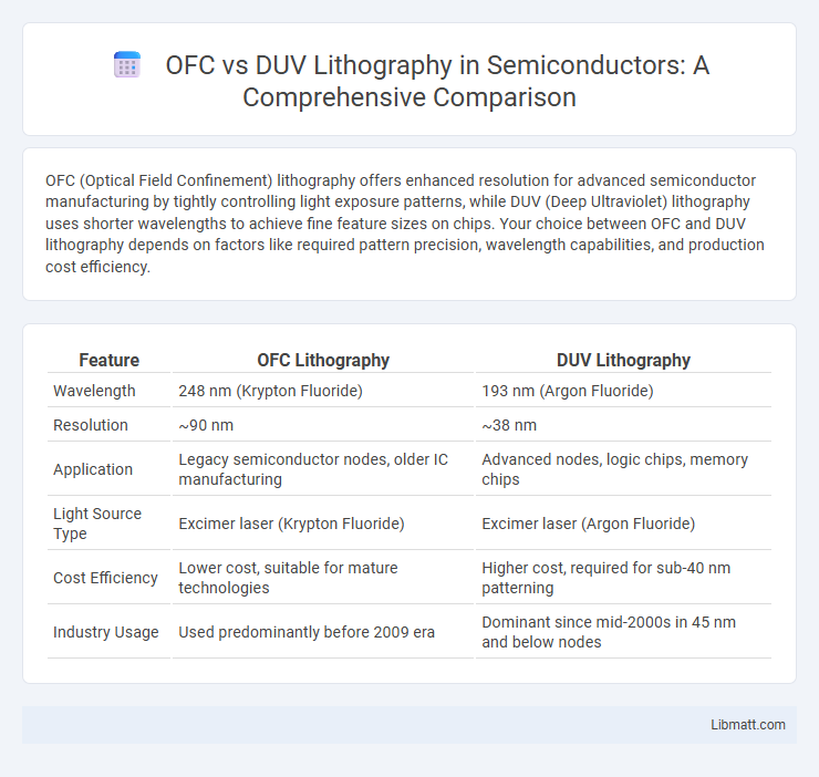
Table of Comparison
| Feature | OFC Lithography | DUV Lithography |
|---|---|---|
| Wavelength | 248 nm (Krypton Fluoride) | 193 nm (Argon Fluoride) |
| Resolution | ~90 nm | ~38 nm |
| Application | Legacy semiconductor nodes, older IC manufacturing | Advanced nodes, logic chips, memory chips |
| Light Source Type | Excimer laser (Krypton Fluoride) | Excimer laser (Argon Fluoride) |
| Cost Efficiency | Lower cost, suitable for mature technologies | Higher cost, required for sub-40 nm patterning |
| Industry Usage | Used predominantly before 2009 era | Dominant since mid-2000s in 45 nm and below nodes |
Introduction to OFC and DUV Lithography
Optical lithography employs Deep Ultraviolet (DUV) light sources with wavelengths typically around 193 nm to pattern microchips, enabling high-resolution semiconductor fabrication. Optical Fiber Communication (OFC) lithography, although less common in the semiconductor context, often refers to techniques utilizing optical fibers for precise light delivery in microfabrication processes. DUV lithography remains the industry standard for advanced node semiconductor manufacturing due to its superior resolution and pattern fidelity compared to conventional optical methods.
What is OFC Lithography?
OFC lithography, or Optical Frontside Coating lithography, is a semiconductor fabrication technique that enhances pattern fidelity by applying a specialized optical coating to the wafer surface. This method reduces reflections and improves light absorption during the photolithography process, resulting in finer feature resolution compared to traditional lithography methods like DUV (Deep Ultraviolet) lithography. OFC lithography is particularly beneficial in manufacturing advanced integrated circuits where precise patterning at the nanoscale is critical.
What is DUV Lithography?
DUV Lithography, or Deep Ultraviolet Lithography, uses light with wavelengths between 200-300 nanometers to pattern intricate semiconductor circuits on silicon wafers. This technology supports feature sizes down to 22 nanometers, making it essential for advanced microchip manufacturing. Understanding DUV Lithography helps you evaluate semiconductor fabrication processes and their impact on device performance.
Key Differences Between OFC and DUV Lithography
OFC (Optical Fiber Communication) lithography uses deep ultraviolet (DUV) light sources but is primarily designed for high-resolution patterning in semiconductor manufacturing, whereas traditional DUV lithography employs ultraviolet light in the 193-248 nm range for photolithography processes. The key differences lie in the wavelength precision, resolution capability, and application focus--OFC lithography offers enhanced resolution and patterning accuracy ideal for nanoscale semiconductor features, while DUV lithography remains widely used for standard feature sizes. Your choice between OFC and DUV lithography depends on the required feature size, throughput, and production cost constraints in semiconductor fabrication.
Technical Principles: OFC vs DUV
Optical Frequency Comb (OFC) lithography employs a spectrum of discrete, equally spaced frequencies generated by mode-locked lasers, enabling ultra-precise wavelength control and enhanced resolution beyond traditional limits. Deep Ultraviolet (DUV) lithography uses fixed-wavelength light sources, typically around 193 nm, relying on high numerical aperture optics and photoresist chemistry to achieve fine feature patterning on semiconductor wafers. Your choice between OFC and DUV lithography depends on the need for extreme spectral precision and minimized diffraction effects offered by OFC versus the mature, high-throughput capabilities of established DUV systems.
Applications in Semiconductor Manufacturing
OFC (Optical Fiber Communication) lithography is critical for producing high-speed, low-loss optical interconnects within semiconductor devices, optimizing data transmission in photonic integrated circuits. DUV (Deep Ultraviolet) lithography dominates the fabrication of advanced logic and memory chips, enabling feature sizes down to 22nm through wavelengths near 193nm, essential for high-density transistor patterning. Both technologies are integral in semiconductor manufacturing, with OFC focusing on optical device precision and DUV advancing miniaturization in electronic circuit fabrication.
Advantages and Limitations of OFC Lithography
OFC lithography offers superior pattern precision and reduced light diffraction compared to DUV lithography, enabling the production of smaller, more intricate semiconductor features essential for advanced microchips. Its advantages include higher resolution and enhanced depth of focus, which improve overall device performance and yield. Limitations of OFC lithography involve higher equipment costs, complex process integration, and sensitivity to environmental factors, making it less accessible for large-scale manufacturing compared to the more established DUV technology.
Advantages and Limitations of DUV Lithography
Deep Ultraviolet (DUV) lithography offers high throughput and cost-effectiveness, making it suitable for manufacturing semiconductor devices with feature sizes down to 22nm. It benefits from mature technology and widespread industry adoption, enabling efficient production at large scales. However, DUV lithography faces limitations in resolution due to its longer wavelength compared to Extreme Ultraviolet (EUV), requiring complex multiple patterning techniques to achieve smaller geometries, which increases process complexity and cost.
Cost and Scalability Analysis
OFC lithography offers lower initial equipment costs and simpler maintenance, making it cost-effective for small to medium production volumes, while DUV lithography involves higher capital expenditure but supports greater throughput and finer resolution essential for large-scale semiconductor manufacturing. Scalability favors DUV lithography due to its compatibility with advanced node technology and higher wafer processing speeds, enabling better yield management as production demands increase. Your choice between OFC and DUV lithography should consider volume requirements and long-term cost efficiency in wafer fabrication.
Future Trends: OFC and DUV Lithography
Future trends in OFC and DUV lithography emphasize increased resolution and cost-effectiveness with ongoing advancements in optical materials and laser technologies. OFC lithography is expected to benefit from improved light sources and mask technologies, enhancing precision for semiconductor manufacturing at smaller nodes. DUV lithography continues evolving with enhanced immersion techniques and multi-patterning strategies to extend its applicability before extreme ultraviolet (EUV) lithography becomes dominant.
OFC vs DUV Lithography Infographic