The lift-off process creates patterned thin films by depositing material over a resist and then removing the resist to leave the desired structure intact, offering sharp edges and clean patterns ideal for delicate features. Etch-back process removes excess material through controlled etching, which can achieve planar surfaces but may cause slight undercutting or roughness, affecting your device's overall precision depending on the application.
Table of Comparison
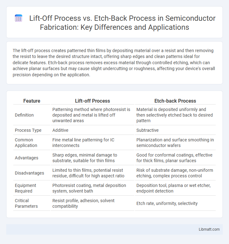
| Feature | Lift-off Process | Etch-back Process |
|---|---|---|
| Definition | Patterning method where photoresist is deposited and metal is lifted off unwanted areas | Material is deposited uniformly and then selectively etched back to desired pattern |
| Process Type | Additive | Subtractive |
| Common Application | Fine metal line patterning for IC interconnects | Planarization and surface smoothing in semiconductor wafers |
| Advantages | Sharp edges, minimal damage to substrate, suitable for thin films | Good for conformal coatings, effective for thick films, planar surfaces |
| Disadvantages | Limited to thin films, potential resist residue, difficult for high aspect ratio | Risk of substrate damage, non-uniform etching, complex process control |
| Equipment Required | Photoresist coating, metal deposition system, solvent bath | Deposition tool, plasma or wet etcher, endpoint detection |
| Critical Parameters | Resist profile, adhesion, solvent compatibility | Etch rate, uniformity, selectivity |
Introduction to Semiconductor Patterning Techniques
Lift-off process and etch-back process are key semiconductor patterning techniques used to create precise micro-scale structures on wafers. Lift-off involves depositing a material over a patterned resist and then removing the resist to leave the desired pattern, ideal for metals and delicate layers. Etch-back uses anisotropic or isotropic etching to remove excess material and reveal underlying features, offering high control for planarization and pattern definition in device fabrication.
Overview of Lift-off Process
The lift-off process involves depositing a sacrificial resist layer patterned on a substrate, followed by the evaporation or sputtering of the desired material. After deposition, the resist layer is dissolved, removing unwanted material and leaving behind a precise patterned film. This technique is particularly effective for creating fine metal patterns and is widely used in microfabrication and semiconductor device manufacturing.
Overview of Etch-back Process
The etch-back process is a technique used in semiconductor manufacturing to planarize thin films by selectively removing excess material via controlled etching. This method improves surface uniformity, ensuring better device performance and reliability, especially in integrated circuit fabrication. Your choice of etch-back over lift-off depends on the specific patterning precision, material compatibility, and process requirements.
Key Steps in the Lift-off Method
The Lift-off Process involves coating the substrate with a resist layer, patterning it using photolithography, and depositing the desired material over the resist. After deposition, the resist is dissolved, lifting off unwanted material and leaving the patterned film on the substrate. This method is ideal for creating precise microstructures and fine metal patterns without etching the underlying layers.
Key Steps in the Etch-back Method
The Etch-back Process involves depositing a conformal film over the wafer, followed by anisotropic etching to remove the film from top surfaces while leaving material in recesses. Precise control of etch rate and uniformity is critical to ensure selective removal without damaging underlying structures. This method is widely used for planarization and pattern definition in semiconductor fabrication, offering superior step coverage compared to the lift-off process.
Material Compatibility and Selection
The lift-off process enables patterning of materials that are sensitive to etchants, such as metals like gold, platinum, and aluminum, preserving their integrity during fabrication. In contrast, the etch-back process requires materials that can withstand selective etching chemicals, limiting compatibility to robust dielectrics and certain metals like silicon dioxide and tungsten. Material selection in lift-off favors metals with poor etch resistance, while etch-back suits applications demanding precise thickness control of hard, etch-resistant films.
Process Advantages and Disadvantages
The Lift-off process excels in patterning metals on sensitive substrates without etching damage, offering high-resolution definition and compatibility with complex topographies, but struggles with poor adhesion and challenges in achieving clean edges on thick films. The Etch-back process provides superior uniformity and excellent step coverage, ideal for achieving planar surfaces in semiconductor fabrication, though it involves longer processing times and risk of substrate damage due to aggressive etching chemicals. Both techniques require careful consideration of material compatibility and process control to optimize device performance and yield.
Common Applications in Microfabrication
The lift-off process is commonly employed in microfabrication for patterning metals in thin-film deposition, especially in applications like photonic devices, MEMS, and integrated circuits where precise metal pattern definition is critical. The etch-back process is preferred for creating planar surfaces and feature size control in microelectronics and MEMS fabrication, often used in applications like dielectric polishing, thin-film planarization, and pattern transfer. Both processes optimize device performance by enabling targeted material removal or deposition in semiconductor manufacturing and nanofabrication industries.
Challenges and Limitations
The Lift-off Process struggles with achieving clean edge definitions and often results in residue or metal stringers due to incomplete resist removal, which limits its effectiveness for fine feature patterning below 1 um. In contrast, the Etch-back Process faces challenges like substrate damage and non-uniform etching rates that can compromise film integrity and thickness uniformity. Both methods demand precise control over process parameters to mitigate defects, but lift-off is generally more suitable for thick metal layers, whereas etch-back excels in planarization but with increased risk of surface roughness.
Choosing Between Lift-off and Etch-back Processes
Choosing between lift-off and etch-back processes depends on factors such as feature size, material compatibility, and process complexity. Lift-off is ideal for patterning thin metal films on sensitive substrates with minimal damage, offering higher resolution for fine structures but limited film thickness. Etch-back is preferred for planarization and thicker film deposition, providing better step coverage but requiring careful etch selectivity and substrate tolerance to avoid damage.
Lift-off Process vs Etch-back Process Infographic