FOWLP (Fan-Out Wafer-Level Packaging) offers enhanced electrical performance and reduced packaging size by redistributing I/O connections without the need for a substrate, making it ideal for high-density applications. FC-CSP (Flip-Chip Chip Scale Package) provides excellent mechanical stability and thermal performance through direct chip attachment to the substrate, suitable for applications demanding robust heat dissipation and reliability.
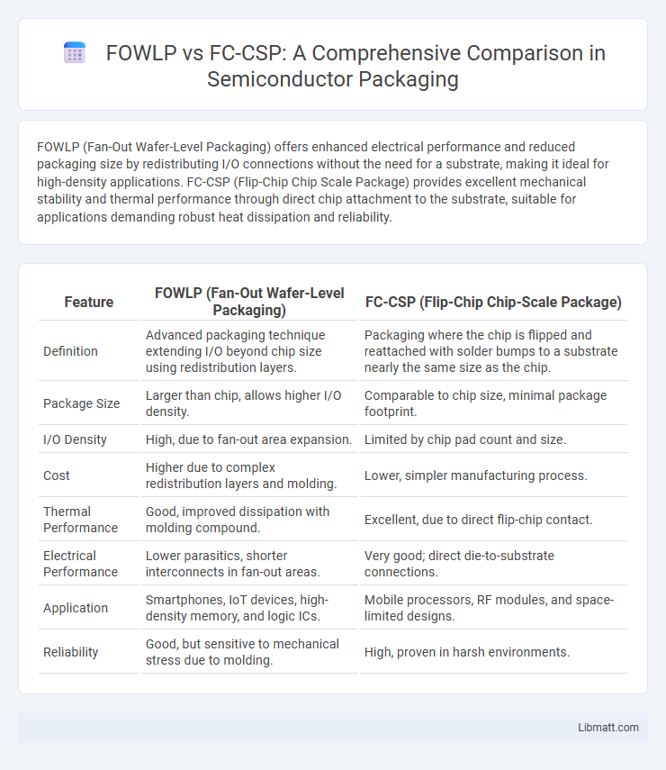
Table of Comparison
| Feature | FOWLP (Fan-Out Wafer-Level Packaging) | FC-CSP (Flip-Chip Chip-Scale Package) |
|---|---|---|
| Definition | Advanced packaging technique extending I/O beyond chip size using redistribution layers. | Packaging where the chip is flipped and reattached with solder bumps to a substrate nearly the same size as the chip. |
| Package Size | Larger than chip, allows higher I/O density. | Comparable to chip size, minimal package footprint. |
| I/O Density | High, due to fan-out area expansion. | Limited by chip pad count and size. |
| Cost | Higher due to complex redistribution layers and molding. | Lower, simpler manufacturing process. |
| Thermal Performance | Good, improved dissipation with molding compound. | Excellent, due to direct flip-chip contact. |
| Electrical Performance | Lower parasitics, shorter interconnects in fan-out areas. | Very good; direct die-to-substrate connections. |
| Application | Smartphones, IoT devices, high-density memory, and logic ICs. | Mobile processors, RF modules, and space-limited designs. |
| Reliability | Good, but sensitive to mechanical stress due to molding. | High, proven in harsh environments. |
Introduction to FOWLP and FC-CSP
Fan-Out Wafer-Level Packaging (FOWLP) offers a cost-effective solution with improved electrical performance by redistributing chip I/O connections beyond the chip's original footprint using a mold compound. Flip-Chip Chip-Scale Package (FC-CSP) places tiny solder bumps directly on the chip, enabling a compact size and enhanced thermal management by attaching the die to the substrate face-down. Your choice between FOWLP and FC-CSP depends on design requirements such as package size, electrical performance, and thermal considerations.
Overview of Advanced Semiconductor Packaging
FoWLP (Fan-Out Wafer-Level Packaging) offers a thin, high-density interconnect solution by redistributing I/O beyond the chip footprint, enhancing electrical performance and thermal management. FC-CSP (Flip-Chip Chip-Scale Package) provides compact, low-inductance connections through direct chip-to-substrate solder bump integration, optimizing signal integrity for high-speed applications. Your choice between FoWLP and FC-CSP depends on specific device requirements like package size, electrical performance, and manufacturing cost constraints in advanced semiconductor packaging.
Key Differences Between FOWLP and FC-CSP
FOWLP (Fan-Out Wafer-Level Packaging) offers a substrate-like redistribution layer without a traditional package substrate, enabling higher I/O density and improved electrical performance compared to FC-CSP (Flip-Chip Chip-Scale Package), which relies on a chip-on-substrate approach. FOWLP provides a thinner profile and better thermal dissipation due to its wafer-level processing, whereas FC-CSP is limited by substrate thickness and can experience higher thermal resistance. Cost efficiency of FOWLP rises with complex, high-pin-count devices, while FC-CSP remains suitable for simpler, lower I/O applications due to its established manufacturing processes.
FOWLP: Structure and Process Flow
FOWLP (Fan-Out Wafer-Level Packaging) features a structure where individual dies are embedded in a mold compound and redistributed with fan-out interconnections, enabling higher I/O density and improved electrical performance. The process flow involves wafer thinning, die singulation, molding, redistribution layer formation, and final bumping for board-level integration. Your selection should consider FOWLP's advantages in miniaturization and thermal management compared to FC-CSP (Flip-Chip Chip-Scale Package).
FC-CSP: Structure and Process Flow
FC-CSP (Fan-Out Chip Scale Package) features a structure where the chip is embedded in a molded resin with redistributed layers spreading outwards to enhance wiring density and thermal performance. Its process flow includes die placement on a temporary carrier, molding with epoxy resin, redistribution layer (RDL) formation, and finally, wafer-level testing before singulation. This packaging technique offers improved electrical performance and miniaturization advantages compared to traditional FOWLP (Fan-Out Wafer Level Packaging).
Performance Comparison: FOWLP vs FC-CSP
FOWLP (Fan-Out Wafer-Level Packaging) offers superior electrical performance with shorter interconnects and reduced parasitic inductance compared to FC-CSP (Flip-Chip Chip Scale Package), enhancing signal integrity and overall device speed. FC-CSP provides a more straightforward manufacturing process and cost benefits but may exhibit higher resistance and capacitance, potentially limiting high-frequency performance. Evaluating your application's frequency range and power requirements is crucial to determine whether FOWLP's advanced performance advantages outweigh FC-CSP's simplicity and cost-effectiveness.
Cost Analysis and Manufacturing Complexity
FOWLP (Fan-Out Wafer-Level Packaging) generally offers lower manufacturing costs compared to FC-CSP (Flip-Chip Chip-Scale Packaging) due to reduced substrate usage and simpler assembly processes. However, FC-CSP can present less complexity in terms of patterning and alignment, benefiting high-volume production with established workflows. Your choice between these options should consider budget constraints and production scale, balancing cost efficiency against manufacturing intricacies.
Application Areas for FOWLP and FC-CSP
FOWLP (Fan-Out Wafer-Level Packaging) is widely applied in smartphones, IoT devices, and high-performance computing due to its excellent electrical performance and compact form factor. FC-CSP (Flip-Chip Chip-Scale Packaging) is commonly used in consumer electronics, automotive systems, and medical devices, offering robust thermal management and reliable power delivery. Your choice between FOWLP and FC-CSP should be guided by specific application requirements such as miniaturization, performance, and environmental conditions.
Future Trends in Advanced Packaging Technologies
FOWLP (Fan-Out Wafer-Level Packaging) offers superior electrical performance and heat dissipation compared to FC-CSP (Flip-Chip Chip Scale Package), making it a preferred choice for future semiconductor devices. As device miniaturization accelerates, FOWLP's ability to support high-density interconnections and improved form factors drives industry adoption for 5G, AI, and IoT applications. Your development strategy should incorporate FOWLP to leverage these scalable, cost-effective packaging solutions that address the evolving demands of advanced packaging technologies.
Choosing the Right Packaging: FOWLP or FC-CSP?
Fan-Out Wafer-Level Packaging (FOWLP) offers enhanced electrical performance, reduced package size, and improved thermal management compared to Flip Chip Chip Scale Package (FC-CSP), making it ideal for applications demanding high integration and miniaturization. FC-CSP remains advantageous for cost-sensitive, high-volume production due to its mature manufacturing process and robust mechanical reliability. Selecting between FOWLP and FC-CSP depends on specific requirements such as design complexity, thermal constraints, package density, and overall cost objectives.
FOWLP vs FC-CSP Infographic