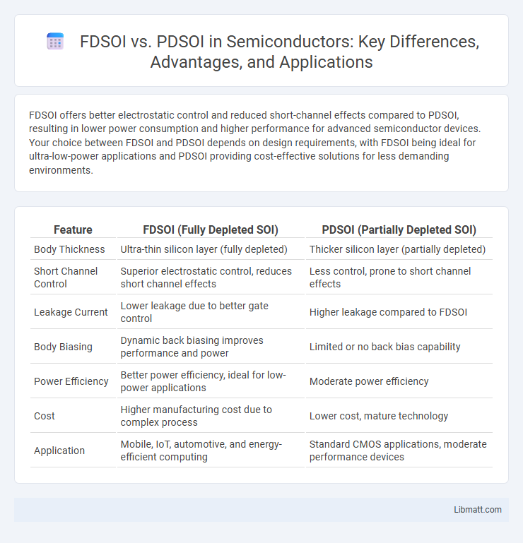
FDSOI offers better electrostatic control and reduced short-channel effects compared to PDSOI, resulting in lower power consumption and higher performance for advanced semiconductor devices. Your choice between FDSOI and PDSOI depends on design requirements, with FDSOI being ideal for ultra-low-power applications and PDSOI providing cost-effective solutions for less demanding environments.
Table of Comparison
| Feature | FDSOI (Fully Depleted SOI) | PDSOI (Partially Depleted SOI) |
|---|---|---|
| Body Thickness | Ultra-thin silicon layer (fully depleted) | Thicker silicon layer (partially depleted) |
| Short Channel Control | Superior electrostatic control, reduces short channel effects | Less control, prone to short channel effects |
| Leakage Current | Lower leakage due to better gate control | Higher leakage compared to FDSOI |
| Body Biasing | Dynamic back biasing improves performance and power | Limited or no back bias capability |
| Power Efficiency | Better power efficiency, ideal for low-power applications | Moderate power efficiency |
| Cost | Higher manufacturing cost due to complex process | Lower cost, mature technology |
| Application | Mobile, IoT, automotive, and energy-efficient computing | Standard CMOS applications, moderate performance devices |
Introduction to SOI Technologies
Fully Depleted Silicon On Insulator (FDSOI) and Partially Depleted Silicon On Insulator (PDSOI) are advanced semiconductor technologies designed to enhance transistor performance by reducing parasitic capacitance and improving speed. FDSOI features a thin silicon layer that is fully depleted of charge carriers, providing better control of short-channel effects and lower power consumption compared to PDSOI, where the silicon layer remains partially depleted. Choosing FDSOI can optimize your device's energy efficiency and scalability, especially for applications requiring low leakage currents and high performance.
Overview of FDSOI and PDSOI
Fully Depleted Silicon-On-Insulator (FDSOI) technology features an ultra-thin silicon layer over a buried oxide that enables enhanced electrostatic control, reduced short-channel effects, and lower leakage currents compared to Partially Depleted SOI (PDSOI). PDSOI uses a thicker silicon layer that is only partially depleted, which can cause parasitic transistor effects and higher leakage but offers simpler manufacturing and design flexibility. FDSOI is preferred for advanced low-power, high-performance applications while PDSOI remains viable in applications tolerant to higher power consumption and variability.
Key Differences Between FDSOI and PDSOI
FDSOI (Fully Depleted Silicon-On-Insulator) features an ultra-thin silicon layer on an insulator, enabling better electrostatic control and significantly reduced leakage currents compared to PDSOI (Partially Depleted Silicon-On-Insulator), which has a thicker silicon layer leading to partial depletion and higher parasitic capacitance. FDSOI offers superior short-channel control and improved performance at lower voltages, making it ideal for energy-efficient and high-speed applications, while PDSOI provides easier fabrication and lower cost but with compromised scaling and power efficiency. Understanding these key differences helps you choose the right technology for optimizing device performance and power consumption in semiconductor design.
Device Architecture: FDSOI vs PDSOI
FDSOI (Fully Depleted Silicon On Insulator) features an ultra-thin silicon layer fully depleted of charge carriers, enabling superior electrostatic control and reduced short-channel effects compared to PDSOI (Partially Depleted Silicon On Insulator), which has a thicker silicon layer with partial depletion. The thin silicon film in FDSOI eliminates floating body effects common in PDSOI, enhancing device stability and reducing leakage currents. FDSOI architecture also allows for dynamic threshold voltage tuning through back biasing, a capability limited or absent in PDSOI designs.
Performance Comparison: Speed and Power Efficiency
Performance comparison between FDSOI (Fully Depleted Silicon On Insulator) and PDSOI (Partially Depleted Silicon On Insulator) reveals that FDSOI offers superior speed due to reduced short-channel effects and improved electrostatic control. FDSOI provides enhanced power efficiency by minimizing leakage currents and enabling aggressive voltage scaling, making it ideal for low-power applications. Your designs can achieve higher performance densities and energy savings using FDSOI technology over PDSOI.
Manufacturing Complexity and Cost
FDSOI (Fully Depleted Silicon-On-Insulator) offers simpler manufacturing processes compared to PDSOI (Partially Depleted SOI) due to its ultrathin body and buried oxide layer, which reduce variability and improve device control. Although FDSOI requires precise thickness control during wafer fabrication, it generally incurs lower overall costs thanks to fewer doping steps and better scalability. Your choice between FDSOI and PDSOI should consider these factors, as FDSOI often delivers cost-effective manufacturing with enhanced performance for advanced semiconductor applications.
Scalability and Technology Nodes
FD-SOI technology offers superior scalability compared to PD-SOI, enabling efficient operation at sub-10nm technology nodes due to its ultra-thin buried oxide and fully depleted channel. PD-SOI struggles with short-channel effects and variability at advanced nodes beyond 22nm, limiting its performance in cutting-edge applications. The inherent electrostatic control in FD-SOI facilitates lower leakage currents and enhanced performance, making it more suitable for future technology node scaling.
Applications and Use Cases
FDSOI technology excels in low-power IoT devices, mobile processors, and wearable electronics due to its superior power efficiency and better control over short-channel effects. PDSOI finds its niche in RF applications, automotive electronics, and mixed-signal circuits where radiation hardness and latch-up immunity are critical. Your choice between FDSOI and PDSOI should align with the specific power, performance, and environmental requirements of your application.
Challenges and Limitations
FDSOI faces challenges such as increased manufacturing complexity and higher costs due to its ultra-thin buried oxide layer requiring precise control. PDSOI suffers from self-heating effects and floating-body phenomena, which can degrade device reliability and limit performance. Your choice between FDSOI and PDSOI must consider these trade-offs in manufacturing yield, thermal management, and device variability.
Future Trends in SOI Technology
FDSOI (Fully Depleted Silicon On Insulator) is gaining momentum over PDSOI (Partially Depleted Silicon On Insulator) due to its superior electrostatic control, lower power consumption, and enhanced performance at nanoscale nodes. Emerging trends in SOI technology emphasize FDSOI's scalability for advanced AI, IoT, and 5G applications, driven by its ability to reduce short-channel effects and improve threshold voltage variability. Your semiconductor designs may benefit from adopting FDSOI to leverage these capabilities for future high-efficiency, low-power integrated circuits.
FDSOI vs PDSOI Infographic