Oxide etching selectively removes silicon dioxide layers using chemicals like hydrofluoric acid or plasma processes, while nitride etching targets silicon nitride films with different etchants such as hot phosphoric acid or specialized plasma recipes. Understanding these distinct etching methods helps you achieve precise patterning and layering in semiconductor fabrication for optimal device performance.
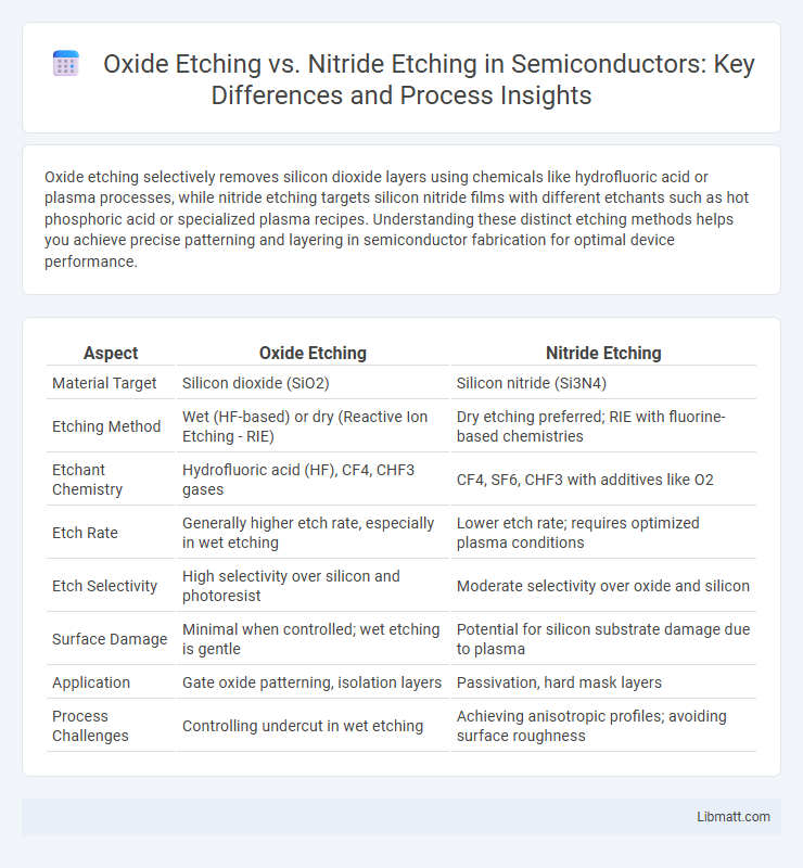
Table of Comparison
| Aspect | Oxide Etching | Nitride Etching |
|---|---|---|
| Material Target | Silicon dioxide (SiO2) | Silicon nitride (Si3N4) |
| Etching Method | Wet (HF-based) or dry (Reactive Ion Etching - RIE) | Dry etching preferred; RIE with fluorine-based chemistries |
| Etchant Chemistry | Hydrofluoric acid (HF), CF4, CHF3 gases | CF4, SF6, CHF3 with additives like O2 |
| Etch Rate | Generally higher etch rate, especially in wet etching | Lower etch rate; requires optimized plasma conditions |
| Etch Selectivity | High selectivity over silicon and photoresist | Moderate selectivity over oxide and silicon |
| Surface Damage | Minimal when controlled; wet etching is gentle | Potential for silicon substrate damage due to plasma |
| Application | Gate oxide patterning, isolation layers | Passivation, hard mask layers |
| Process Challenges | Controlling undercut in wet etching | Achieving anisotropic profiles; avoiding surface roughness |
Introduction to Oxide and Nitride Etching
Oxide etching primarily targets silicon dioxide (SiO2) layers using fluorine-based plasmas such as CF4 or CHF3, enabling precise pattern transfer in semiconductor fabrication. Nitride etching focuses on silicon nitride (Si3N4) films, often employing chlorine or fluorine chemistries like Cl2 or SF6 to achieve selective material removal with minimal substrate damage. Both processes are critical in microfabrication, with etching selectivity, rate, and profile control being key parameters that differ according to the chemical and physical properties of oxide and nitride materials.
Fundamental Differences Between Oxide and Nitride Etching
Oxide etching primarily targets silicon dioxide (SiO2) layers, using chemistry that selectively removes oxide with high precision, often employing hydrofluoric acid (HF) or plasma containing fluorine species. Nitride etching focuses on silicon nitride (Si3N4), requiring different chemistries such as hot phosphoric acid or fluorocarbon-based plasmas to effectively break its stronger chemical bonds and achieve anisotropic profiles. Understanding the fundamental differences in etch rates, selectivity, and chemical reactions helps optimize your semiconductor fabrication processes for either oxide or nitride layers.
Material Properties: Oxides vs Nitrides
Oxide etching targets silicon dioxide, a material known for its excellent electrical insulation and lower hardness compared to silicon nitride, which exhibits superior chemical resistance and mechanical strength. Nitride etching requires more aggressive chemistries due to silicon nitride's dense bonding structure and higher etch selectivity needs. Understanding these material properties helps optimize your etching process for precision and efficiency in semiconductor manufacturing.
Common Applications of Oxide Etching
Oxide etching is widely used in semiconductor manufacturing for patterning silicon dioxide layers in integrated circuits and microelectromechanical systems (MEMS). It plays a crucial role in processes such as gate oxide removal, contact hole formation, and shallow trench isolation (STI) during chip fabrication. Advanced techniques like reactive ion etching (RIE) enable precise control over oxide layer thickness and etch profiles, essential for high-performance device reliability.
Common Applications of Nitride Etching
Nitride etching is commonly applied in semiconductor manufacturing for creating precise silicon nitride mask layers used in microelectromechanical systems (MEMS) and integrated circuits (ICs). It is essential for wafer passivation, dielectric patterning, and surface planarization due to its high selectivity and anisotropic etching properties. These characteristics enable effective layer definition in advanced CMOS technology and thin-film transistor (TFT) fabrication.
Etching Methods: Wet vs Dry Techniques
Oxide etching commonly employs both wet techniques, using hydrofluoric acid solutions, and dry methods such as plasma etching with fluorocarbon gases, offering high precision and selective removal. Nitride etching typically relies on dry plasma processes using gases like CF4, CHF3, or SF6 to achieve anisotropic profiles essential for device fabrication. Wet etching of nitride is less favored due to poor selectivity and control, making dry etching the preferred choice for nitride patterning in semiconductor manufacturing.
Selectivity and Precision in Etching Processes
Oxide etching exhibits high selectivity when removing silicon dioxide layers while preserving underlying materials, making it ideal for precise pattern transfer in CMOS fabrication. Nitride etching requires carefully tuned chemistry to achieve sharp anisotropic profiles and avoid damaging adjacent oxide or silicon layers, demanding superior control over plasma parameters. Your choice between oxide and nitride etching will significantly impact process precision and selectivity, influencing overall device performance and yield.
Challenges and Solutions in Oxide Etching
Oxide etching presents challenges such as selectivity control, uniformity, and damage to underlying layers due to its chemical inertness and high etch rates. Advanced plasma chemistries and endpoint detection techniques enhance precision, while process optimization minimizes substrate damage, ensuring better control over feature profiles. Your oxide etching process benefits from integrating real-time monitoring and adaptive parameters to overcome these complexities effectively.
Challenges and Solutions in Nitride Etching
Nitride etching presents challenges such as selectivity control, anisotropy, and surface roughness due to the chemical stability of silicon nitride compared to oxide. Solutions involve optimizing plasma chemistry with fluorine-based gases combined with passivation techniques using additives like hydrogen or oxygen to enhance etch profile and reduce damage. Advanced process control methods including real-time endpoint detection and chamber conditioning improve consistency and minimize defects during nitride patterning.
Future Trends in Oxide and Nitride Etching Technologies
Future trends in oxide and nitride etching technologies emphasize enhanced precision and selectivity through advanced plasma and atomic layer etching techniques. Emerging methods integrate real-time endpoint detection and AI-driven process control to optimize etch profiles and reduce defects in semiconductor manufacturing. You can expect continuous innovation targeting lower damage, higher throughput, and compatibility with next-generation materials for improved device performance.
Oxide Etching vs Nitride Etching Infographic