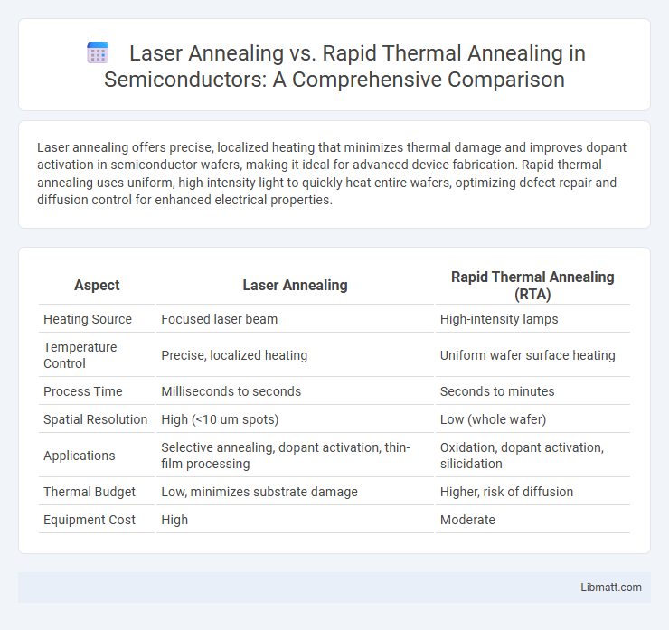
Laser annealing offers precise, localized heating that minimizes thermal damage and improves dopant activation in semiconductor wafers, making it ideal for advanced device fabrication. Rapid thermal annealing uses uniform, high-intensity light to quickly heat entire wafers, optimizing defect repair and diffusion control for enhanced electrical properties.
Table of Comparison
| Aspect | Laser Annealing | Rapid Thermal Annealing (RTA) |
|---|---|---|
| Heating Source | Focused laser beam | High-intensity lamps |
| Temperature Control | Precise, localized heating | Uniform wafer surface heating |
| Process Time | Milliseconds to seconds | Seconds to minutes |
| Spatial Resolution | High (<10 um spots) | Low (whole wafer) |
| Applications | Selective annealing, dopant activation, thin-film processing | Oxidation, dopant activation, silicidation |
| Thermal Budget | Low, minimizes substrate damage | Higher, risk of diffusion |
| Equipment Cost | High | Moderate |
Introduction to Thermal Annealing Techniques
Thermal annealing techniques like Laser Annealing and Rapid Thermal Annealing (RTA) are essential for modifying material properties through controlled heat treatment. Laser Annealing offers precise, localized heating with rapid cooling rates ideal for semiconductor fabrication, while RTA provides uniform temperature profiles for stress relief and dopant activation across entire wafers. Your choice depends on required resolution, thermal budget, and material compatibility in advanced manufacturing processes.
What is Laser Annealing?
Laser annealing is a semiconductor fabrication process that uses a high-intensity laser beam to rapidly heat the surface of a material, altering its physical and electrical properties without affecting the bulk substrate. Unlike rapid thermal annealing (RTA), which heats the entire wafer uniformly using lamps, laser annealing offers precise, localized control, enabling ultra-fast thermal cycles and minimizing thermal budget. You can achieve enhanced dopant activation and improved crystal quality while reducing diffusion and damage in semiconductor devices through laser annealing.
What is Rapid Thermal Annealing?
Rapid Thermal Annealing (RTA) is a semiconductor manufacturing process that rapidly heats silicon wafers to high temperatures, typically between 600degC and 1200degC, for short durations ranging from a few seconds to minutes. This technique enhances dopant activation and repairs crystal damage without causing significant diffusion, critical for scaling down device features. RTA provides precise thermal control and uniformity, enabling improved electrical performance and reduced thermal budget compared to conventional furnace annealing methods.
Core Principles: Laser vs Rapid Thermal Annealing
Laser annealing uses focused, high-intensity laser pulses to precisely heat the material's surface, enabling ultra-fast thermal processing with minimal impact on underlying layers. Rapid thermal annealing (RTA) uniformly heats the entire wafer using intense lamps or heaters, achieving rapid temperature ramps and short dwell times for overall thermal treatment. Your choice between laser and rapid thermal annealing depends on the desired precision, thermal budget, and material sensitivity during semiconductor fabrication.
Equipment and Process Differences
Laser annealing utilizes high-intensity laser beams for localized, ultra-fast heating, allowing precise control over annealing areas without affecting the entire substrate, whereas rapid thermal annealing (RTA) employs broad-spectrum lamps to rapidly heat the entire wafer uniformly in a controlled atmosphere. Laser annealing equipment typically includes high-power lasers, scanning systems, and advanced beam shaping optics, while RTA setups consist of quartz heating chambers with infrared lamps and precise temperature controllers. The key process difference lies in laser annealing's ability to achieve shallow junction activation with minimal thermal budget, contrasting with RTA's approach of rapid but bulk heating to reduce diffusion and oxidation effects.
Advantages of Laser Annealing
Laser annealing offers precise localized heating, minimizing thermal diffusion and reducing damage to surrounding materials. It enables ultrafast processing times and is compatible with temperature-sensitive substrates, enhancing throughput and device performance. The technique improves dopant activation and junction depth control compared to rapid thermal annealing.
Benefits of Rapid Thermal Annealing
Rapid Thermal Annealing (RTA) offers precise control of temperature and annealing time, enabling uniform dopant activation and minimizing diffusion in semiconductor fabrication. This technique significantly enhances device performance by reducing thermal budget and improving electrical characteristics, such as carrier mobility and junction depth. RTA's compatibility with silicon-based materials and scalability for high-volume manufacturing makes it a preferred choice over Laser Annealing for consistent and reproducible annealing processes.
Applications in Semiconductor Manufacturing
Laser annealing offers precise, localized heating ideal for doping and activating ultra-shallow junctions in advanced semiconductor devices, enhancing performance in high-speed transistors. Rapid Thermal Annealing (RTA) provides uniform, controlled temperature profiles suitable for oxidation, diffusion, and stress relief in wafer-level processing, supporting large-scale production. You can leverage laser annealing for fine-tuned component adjustments, while RTA remains essential for general wafer treatment and bulk semiconductor fabrication.
Limitations and Challenges of Each Method
Laser annealing offers precise, localized heating but struggles with uniformity over large areas and high equipment costs, which can limit scalability for industrial applications. Rapid thermal annealing (RTA) provides faster heating and broader wafer coverage but often faces challenges like thermal stress and limited control over ramp-up and cool-down rates, potentially impacting material quality. Your choice depends on balancing the need for precision versus throughput, considering these inherent limitations and process constraints.
Choosing the Optimal Annealing Technique
Laser Annealing offers precise, localized heating with ultra-fast processing times, making it ideal for applications requiring minimal thermal diffusion and high spatial resolution. Rapid Thermal Annealing provides uniform temperature ramps over entire wafers, suitable for large-scale semiconductor manufacturing where consistent annealing and high throughput are critical. Your choice depends on the material properties, device architecture, and production scale to achieve optimal electronic performance and process efficiency.
Laser Annealing vs Rapid Thermal Annealing Infographic