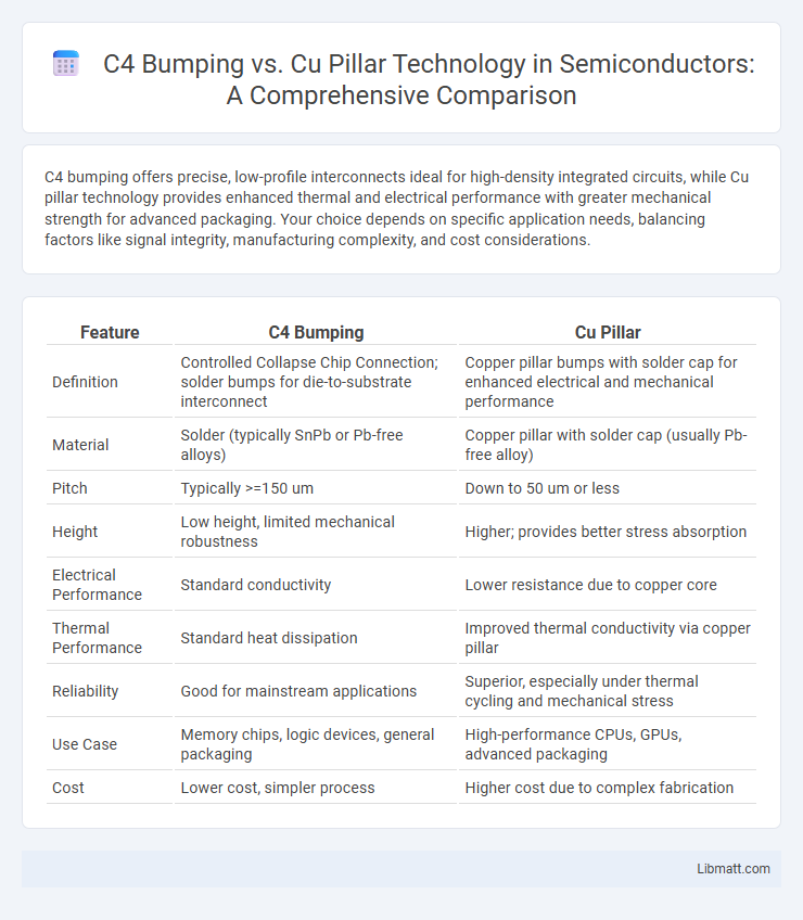
C4 bumping offers precise, low-profile interconnects ideal for high-density integrated circuits, while Cu pillar technology provides enhanced thermal and electrical performance with greater mechanical strength for advanced packaging. Your choice depends on specific application needs, balancing factors like signal integrity, manufacturing complexity, and cost considerations.
Table of Comparison
| Feature | C4 Bumping | Cu Pillar |
|---|---|---|
| Definition | Controlled Collapse Chip Connection; solder bumps for die-to-substrate interconnect | Copper pillar bumps with solder cap for enhanced electrical and mechanical performance |
| Material | Solder (typically SnPb or Pb-free alloys) | Copper pillar with solder cap (usually Pb-free alloy) |
| Pitch | Typically >=150 um | Down to 50 um or less |
| Height | Low height, limited mechanical robustness | Higher; provides better stress absorption |
| Electrical Performance | Standard conductivity | Lower resistance due to copper core |
| Thermal Performance | Standard heat dissipation | Improved thermal conductivity via copper pillar |
| Reliability | Good for mainstream applications | Superior, especially under thermal cycling and mechanical stress |
| Use Case | Memory chips, logic devices, general packaging | High-performance CPUs, GPUs, advanced packaging |
| Cost | Lower cost, simpler process | Higher cost due to complex fabrication |
Introduction to C4 Bumping and Cu Pillar Technologies
C4 bumping involves creating controlled collapse chip connections with solder bumps that enable high-density interconnects in semiconductor packaging, while Cu pillar technology employs copper pillars topped with solder caps to enhance electrical performance and thermal conductivity. Both technologies cater to advanced integrated circuit packaging by improving signal integrity and mechanical reliability, essential for high-speed and high-power applications. Your choice between C4 bumping and Cu pillar depends on specific device requirements such as pitch size, thermal management, and electrical performance needs.
Historical Evolution: From C4 to Cu Pillar
C4 bumping marked a significant milestone in semiconductor packaging by enabling reliable interconnections through solder bumps, but limitations in pitch size and electromigration led to the development of Cu pillar technology. Cu pillar interconnects evolved as a more advanced solution with finer pitch capabilities, superior mechanical strength, and enhanced electrical performance, meeting the demands of modern miniaturized devices. Your designs benefit from Cu pillar's improved scalability and reliability, reflecting the ongoing evolution from traditional C4 bumping to next-generation chip packaging.
Key Differences Between C4 Bumping and Cu Pillar
C4 bumping involves creating solder bumps on semiconductor wafers for flip-chip packaging, enabling efficient electrical connections with high thermal performance. Cu pillar technology uses copper posts capped with solder, offering superior mechanical strength and finer pitch capability compared to traditional solder bumps. Key differences include material composition, with Cu pillars providing enhanced electromigration resistance and better heat dissipation, while C4 bumps are simpler and cost-effective for standard applications.
Material Composition and Structure
C4 bumping utilizes copper pillars plated with a thin solder cap, combining copper's high electrical conductivity and mechanical strength with the solder's reflow capability for reliable interconnections. Copper pillars in advanced packaging are solid copper columns often topped with a thin solder layer, providing precise height control and superior thermal performance compared to traditional solder bumps. Both structures leverage copper's properties but differ in the solder cap thickness and design complexity, impacting their mechanical robustness and thermal conductivity in semiconductor interconnects.
Manufacturing Processes and Challenges
C4 bumping involves creating small solder bumps on silicon wafers to enable flip-chip packaging, requiring precise photolithography, electroplating, and under-bump metallization processes, while Cu pillar technology uses copper posts with solder caps to improve electrical performance and mechanical reliability. Manufacturing challenges for C4 bumping include controlling bump uniformity and avoiding voids, whereas Cu pillar faces difficulties in managing copper oxidation, ensuring strong adhesion, and minimizing crack formation during thermal cycling. Your choice between the two depends on balancing process complexity with the desired electrical and mechanical performance in advanced semiconductor packaging.
Electrical Performance Comparison
C4 bumping offers superior electrical performance with lower resistance and inductance compared to Cu pillars, enhancing signal integrity in high-speed applications. Cu pillars, while providing mechanical robustness, generally exhibit higher parasitic effects that can impact electrical efficiency in advanced packaging. Evaluating your design's electrical requirements ensures the optimal interconnect choice for maximum performance and reliability.
Reliability and Durability Aspects
C4 bumping offers superior mechanical robustness and thermal cycling resistance compared to Cu pillar technology, enhancing long-term reliability in high-stress environments. Cu pillars provide excellent electrical performance and fine pitch capabilities but may experience increased susceptibility to electromigration and fatigue under extended thermal load. Reliability and durability assessments favor C4 bumping for applications demanding consistent mechanical integrity and thermal stability over the device lifecycle.
Applications in Modern Semiconductor Packaging
C4 bumping and Cu pillar technologies are critical in modern semiconductor packaging, enabling higher interconnect density and improved electrical performance. C4 bumping, with its traditional solder ball approach, excels in applications requiring proven reliability and cost-effectiveness, particularly in high-volume consumer electronics. Cu pillar's finer pitch and superior mechanical strength make it ideal for high-performance computing and mobile devices, where signal integrity and thermal management are paramount for your advanced package designs.
Cost Implications: C4 Bumping vs Cu Pillar
C4 bumping generally incurs lower material and processing costs due to its simpler solder ball formation and established manufacturing infrastructure. Cu pillar technology, while offering superior electrical performance and finer pitch capabilities, demands higher expenses stemming from complex fabrication steps and expensive copper materials. Cost implications of Cu pillar are often justified in high-performance applications, whereas C4 bumping remains cost-effective for standard packaging solutions.
Future Trends and Industry Adoption
C4 bumping technology is advancing with finer pitch capabilities and improved reliability, enabling higher performance in semiconductor packaging for next-generation devices. Cu pillar technology offers superior electrical conductivity and mechanical strength, driving widespread adoption in high-density applications such as 5G and AI processors. Industry trends indicate a gradual shift towards Cu pillars due to cost efficiency and scalability in mass production, while C4 bumping remains critical for legacy systems and specialized use cases.
C4 Bumping vs Cu Pillar Infographic