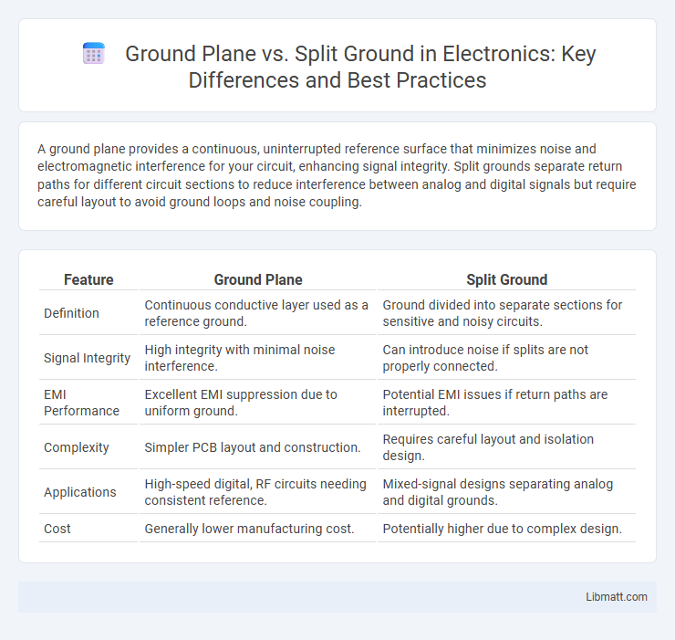
A ground plane provides a continuous, uninterrupted reference surface that minimizes noise and electromagnetic interference for your circuit, enhancing signal integrity. Split grounds separate return paths for different circuit sections to reduce interference between analog and digital signals but require careful layout to avoid ground loops and noise coupling.
Table of Comparison
| Feature | Ground Plane | Split Ground |
|---|---|---|
| Definition | Continuous conductive layer used as a reference ground. | Ground divided into separate sections for sensitive and noisy circuits. |
| Signal Integrity | High integrity with minimal noise interference. | Can introduce noise if splits are not properly connected. |
| EMI Performance | Excellent EMI suppression due to uniform ground. | Potential EMI issues if return paths are interrupted. |
| Complexity | Simpler PCB layout and construction. | Requires careful layout and isolation design. |
| Applications | High-speed digital, RF circuits needing consistent reference. | Mixed-signal designs separating analog and digital grounds. |
| Cost | Generally lower manufacturing cost. | Potentially higher due to complex design. |
Introduction to Ground Plane and Split Ground
A ground plane is a large, continuous conductive surface used in PCB design to provide a low-impedance path for return currents and minimize electromagnetic interference. Split ground refers to dividing the ground plane into separate sections to isolate noisy circuits or sensitive analog signals, enhancing signal integrity. Proper implementation of ground planes and split grounds is crucial for reducing noise and improving overall circuit performance.
Understanding Ground Planes in PCB Design
Ground planes in PCB design provide a low-impedance path for return currents, minimizing noise and interference by creating a uniform reference voltage. Split ground planes, while sometimes necessary to separate analog and digital signals, can introduce signal integrity issues due to discontinuities and increased impedance at splits. Understanding the trade-offs between continuous ground planes and the segmentation in split grounds helps optimize your PCB's electromagnetic compatibility and overall performance.
What is a Split Ground?
A split ground is a PCB design technique where the ground plane is divided into separate sections to isolate noisy or sensitive circuits, minimizing interference and ground noise coupling. This segmentation helps improve signal integrity by preventing current loops and reducing EMI in mixed-signal or high-frequency designs. Unlike a continuous ground plane, split grounds require careful layout to ensure proper grounding and avoid performance degradation.
Key Differences Between Ground Plane and Split Ground
Ground plane designs use a continuous copper layer across the PCB to provide a stable reference voltage and minimize electromagnetic interference (EMI), while split ground involves dividing the ground into separate areas to isolate noise sources and sensitive circuits. Split ground is often preferred in mixed-signal circuits where analog and digital grounds must be separated to reduce interference, whereas ground planes are ideal for high-frequency and RF applications due to their low impedance path. Your choice between ground plane and split ground impacts signal integrity, noise reduction, and overall PCB performance depending on the circuit requirements.
Advantages of a Solid Ground Plane
A solid ground plane offers superior electromagnetic interference (EMI) reduction by providing a continuous low-impedance return path for signals, which enhances signal integrity and minimizes noise. It simplifies PCB layout by reducing ground loops and ensures stable reference voltages across the board, improving overall circuit performance. This approach also facilitates effective heat dissipation and improves high-frequency performance compared to split ground designs.
Benefits and Risks of Split Ground Design
Split ground design improves noise isolation by separating analog and digital grounds, reducing interference in sensitive circuits, which benefits signal integrity in mixed-signal systems. However, improper implementation can create ground loops or potential differences, increasing noise and compromising circuit performance. Your PCB layout must carefully manage return paths to minimize risks and maximize the benefits of split grounds.
Signal Integrity Considerations
Ground plane designs provide a continuous low-inductance return path, minimizing electromagnetic interference and maintaining signal integrity by reducing noise coupling and crosstalk between traces. Split ground configurations, often used for isolating analog and digital sections, can introduce return current discontinuities causing increased impedance and potential signal reflection, degrading high-frequency signal integrity. Careful layout and stitching capacitors are essential to mitigate these effects and ensure stable reference potentials across the PCB.
EMC and Noise Performance Comparison
Ground plane designs provide superior EMC performance by offering a low-impedance path for return currents, minimizing electromagnetic interference and reducing noise coupling across the PCB. Split grounds, while useful for isolating sensitive circuits, can introduce impedance discontinuities that increase EMI and degrade noise performance due to current loop mismatches. Your choice between ground plane and split ground impacts signal integrity and noise resilience, with continuous ground planes generally ensuring better EMC compliance.
Best Practices for Ground Layout
Best practices for ground layout emphasize minimizing noise and interference by using a single, solid ground plane rather than split grounds, which can create ground loops and increase electromagnetic interference (EMI). Ensuring a continuous, low-resistance path for return currents improves signal integrity, especially in high-speed digital and RF circuits. Proper placement of decoupling capacitors and careful routing near ground planes further enhances overall performance by reducing voltage fluctuations and maintaining a stable reference.
When to Use Ground Plane or Split Ground
Ground planes should be used in high-frequency PCB designs to minimize electromagnetic interference (EMI) and provide a low-impedance return path for signals, ensuring signal integrity. Split grounds are ideal when separating analog and digital circuits to reduce noise coupling but require careful layout to avoid creating ground loops and impedance discontinuities. Choosing between ground plane and split ground depends on signal frequency, noise sensitivity, and the need to isolate different circuit sections while maintaining a continuous return path.
Ground plane vs Split ground Infographic