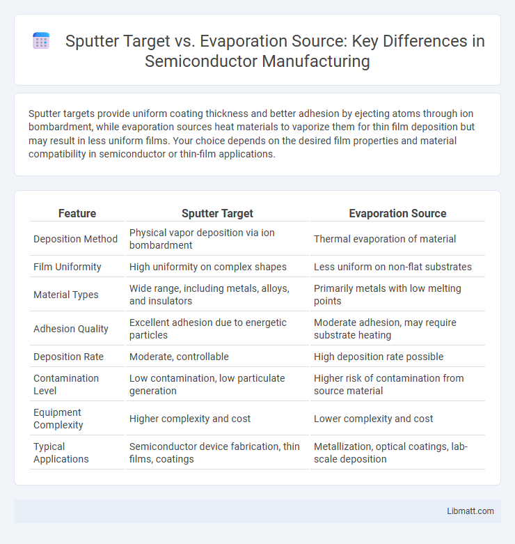
Sputter targets provide uniform coating thickness and better adhesion by ejecting atoms through ion bombardment, while evaporation sources heat materials to vaporize them for thin film deposition but may result in less uniform films. Your choice depends on the desired film properties and material compatibility in semiconductor or thin-film applications.
Table of Comparison
| Feature | Sputter Target | Evaporation Source |
|---|---|---|
| Deposition Method | Physical vapor deposition via ion bombardment | Thermal evaporation of material |
| Film Uniformity | High uniformity on complex shapes | Less uniform on non-flat substrates |
| Material Types | Wide range, including metals, alloys, and insulators | Primarily metals with low melting points |
| Adhesion Quality | Excellent adhesion due to energetic particles | Moderate adhesion, may require substrate heating |
| Deposition Rate | Moderate, controllable | High deposition rate possible |
| Contamination Level | Low contamination, low particulate generation | Higher risk of contamination from source material |
| Equipment Complexity | Higher complexity and cost | Lower complexity and cost |
| Typical Applications | Semiconductor device fabrication, thin films, coatings | Metallization, optical coatings, lab-scale deposition |
Introduction to Thin Film Deposition Methods
Sputter targets and evaporation sources are critical components in thin film deposition, enabling precise material transfer onto substrates for semiconductor, optical, and decorative applications. Sputtering involves ejecting atoms from a solid target using ionized gas, resulting in uniform, high-density films with excellent adhesion and fine control over film composition. Evaporation sources heat materials until they vaporize, depositing atoms in a line-of-sight manner that suits high-purity films but may produce less uniform coverage compared to sputtering techniques.
Understanding Sputter Targets
Sputter targets are essential components in physical vapor deposition (PVD) processes, used to deposit thin films by ejecting atoms from a solid target through ion bombardment. Unlike evaporation sources that rely on thermal energy to vaporize materials, sputter targets enable precise control over film composition and thickness due to their ability to sputter complex alloys and compounds uniformly. The choice of sputter target material directly influences film adhesion, density, and microstructure, making them critical for applications in semiconductor manufacturing, magnetic storage, and optical coatings.
Overview of Evaporation Sources
Evaporation sources are crucial components in thin film deposition, enabling material vaporization through thermal energy for uniform coating applications. Common types include resistive heaters, electron beam evaporators, and induction sources, each offering specific temperature ranges and deposition rates suited for metals, oxides, and polymers. This technique excels in producing high-purity films with precise thickness control, essential for semiconductor, optics, and microelectronics industries.
Material Compatibility and Choices
Sputter targets offer a wider range of material compatibility, including metals, alloys, oxides, and nitrides, making them ideal for complex and multi-layer thin films. Evaporation sources primarily accommodate pure metals and simple compounds, limiting their use with refractory or multi-element materials. The ability of sputter targets to evenly deposit complex materials results in superior film uniformity and stoichiometry control compared to evaporation sources.
Thin Film Quality Comparison
Sputter targets generally produce thin films with superior adhesion, uniformity, and density compared to evaporation sources, resulting in higher-quality coatings for demanding applications. Evaporation sources often lead to films with lower density and more porous microstructures, which can affect the film's electrical and mechanical properties. When precision and film performance are critical, your choice of sputter target improves thin film quality significantly.
Deposition Rate and Efficiency
Sputter targets typically offer higher deposition rates and better material utilization compared to evaporation sources, making them more efficient for large-area coatings and conductive films. Evaporation sources often exhibit lower deposition rates due to their reliance on thermal vaporization, which can lead to material waste and less uniform film thickness. The sputtering process allows for precise control over film density and composition, enhancing overall deposition efficiency in semiconductor and optical coatings.
Equipment Complexity and Cost
Sputter targets typically require more complex and expensive equipment due to the need for ionized gas, magnetic fields, and vacuum chambers to achieve uniform material deposition. Evaporation sources involve simpler setups that use resistive heating or electron beams to vaporize materials, resulting in lower initial costs and maintenance requirements. However, sputtering provides better film uniformity and adhesion, justifying the higher investment in precision applications.
Applications in Industry and Research
Sputter targets are widely utilized in semiconductor manufacturing, thin-film deposition, and advanced coating applications due to their precise control over film composition and uniformity. Evaporation sources are favored in research settings for creating high-purity, low-contamination films and are commonly applied in optical coatings, microelectronics, and material science experiments. Your choice between sputter targets and evaporation sources depends on the specific requirements for film quality, deposition rate, and application environment.
Pros and Cons: Sputter Target vs Evaporation Source
Sputter targets offer uniform thin film deposition with excellent adhesion and better step coverage, making them ideal for complex surface geometries, while evaporation sources provide higher deposition rates and simpler equipment setup but may result in less uniform films and poorer adhesion. Sputtering works well with a wide range of materials, including metals, alloys, and insulators, whereas evaporation is typically limited to materials with lower melting points. When choosing your thin film deposition method, consider sputter targets for precision and durability versus evaporation sources for speed and cost-effectiveness.
Choosing the Right Method for Your Application
Selecting the right thin-film deposition method depends on factors like material type, film uniformity, and adhesion requirements. Sputter targets excel in depositing alloys and compounds with precise thickness control and better film density, making them ideal for semiconductor and optical coatings. Your application benefits from evaporation sources when working with pure metals and simpler materials, offering faster deposition rates and lower equipment costs.
Sputter Target vs Evaporation Source Infographic