EUV (Extreme Ultraviolet) lithography uses a shorter wavelength of 13.5 nm, enabling more precise patterning for advanced semiconductor manufacturing compared to DUV (Deep Ultraviolet) lithography, which typically operates around 193 nm. Choosing EUV technology can significantly enhance your chip design by allowing smaller feature sizes and higher density integration.
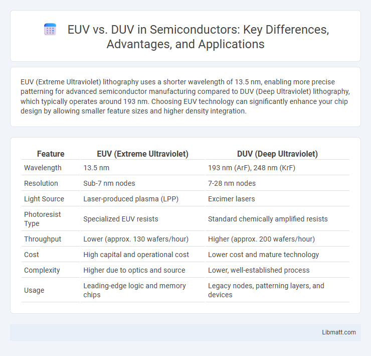
Table of Comparison
| Feature | EUV (Extreme Ultraviolet) | DUV (Deep Ultraviolet) |
|---|---|---|
| Wavelength | 13.5 nm | 193 nm (ArF), 248 nm (KrF) |
| Resolution | Sub-7 nm nodes | 7-28 nm nodes |
| Light Source | Laser-produced plasma (LPP) | Excimer lasers |
| Photoresist Type | Specialized EUV resists | Standard chemically amplified resists |
| Throughput | Lower (approx. 130 wafers/hour) | Higher (approx. 200 wafers/hour) |
| Cost | High capital and operational cost | Lower cost and mature technology |
| Complexity | Higher due to optics and source | Lower, well-established process |
| Usage | Leading-edge logic and memory chips | Legacy nodes, patterning layers, and devices |
Introduction to EUV and DUV Lithography
EUV lithography utilizes extreme ultraviolet light with a wavelength of 13.5 nm to enable semiconductor manufacturing at advanced nodes below 7 nm, significantly enhancing resolution compared to DUV lithography, which operates with wavelengths of 193 nm. DUV lithography remains essential for mature technology nodes and high-volume production due to its reliability and cost-effectiveness. Your choice between EUV and DUV lithography impacts device performance, manufacturing efficiency, and overall chip design complexity.
Defining EUV and DUV: Wavelength Differences
Extreme Ultraviolet (EUV) lithography operates at a wavelength of approximately 13.5 nanometers, enabling the production of semiconductor features below 10 nanometers in size. Deep Ultraviolet (DUV) lithography uses longer wavelengths, typically around 193 nanometers, which limits its resolution capabilities for advanced semiconductor nodes. The significant wavelength difference between EUV and DUV directly impacts the precision and miniaturization potential in semiconductor manufacturing processes.
Historical Evolution of Lithography Technologies
EUV (Extreme Ultraviolet) lithography emerged as a breakthrough technology following decades of advancement in DUV (Deep Ultraviolet) lithography, which dominated semiconductor manufacturing from the 1980s through the early 2010s. DUV lithography, primarily using 193 nm wavelength lasers, became the industry standard for defining critical dimensions below 100 nm through techniques like immersion lithography and multiple patterning. EUV lithography, with its 13.5 nm wavelength light source, was developed to overcome the resolution limits of DUV, enabling finer feature sizes essential for modern semiconductor nodes such as 7 nm and beyond.
Key Applications in Semiconductor Manufacturing
Extreme Ultraviolet (EUV) lithography is primarily used for advanced semiconductor manufacturing nodes below 7nm, enabling the production of high-density integrated circuits with finer feature sizes. Deep Ultraviolet (DUV) lithography remains essential for manufacturing mature nodes above 7nm and serves in fabricating layers that do not require the smallest feature sizes, supporting cost-effective mass production. Both lithography techniques are complementary, with EUV driving innovations in logic chips and memory devices, while DUV continues to optimize yield and throughput for established semiconductor components.
Advantages of EUV Lithography
EUV lithography offers significantly higher resolution compared to DUV, enabling the production of smaller, more complex semiconductor features essential for advanced microchips. It uses a shorter wavelength of 13.5 nm, which allows for finer patterning, enhancing device performance and power efficiency. Your semiconductor manufacturing benefits from reduced mask complexity and fewer process steps, leading to improved yield and lower production costs.
Strengths and Limitations of DUV Lithography
Deep Ultraviolet (DUV) lithography offers strong advantages in cost-effectiveness and established manufacturing processes for semiconductor fabrication, making it ideal for producing chips at feature sizes down to 7nm. Its limitations include difficulty achieving smaller nodes due to resolution constraints and reliance on complex multiple patterning techniques, which increase production complexity and time. Your choice between DUV and EUV depends on balancing the maturity and lower cost of DUV with the need for finer resolution that Extreme Ultraviolet (EUV) lithography provides.
Technical Challenges in EUV vs DUV
EUV lithography faces significant technical challenges compared to DUV, including the generation of high-intensity 13.5 nm wavelength light required for fine patterning that demands complex laser-produced plasma sources. EUV also requires advanced reflective optics with multilayer mirrors to handle extreme wavelengths, addressing issues with absorption and contamination that are less critical in DUV systems operating around 193 nm. Furthermore, EUV masks are more difficult to fabricate and inspect due to their multilayer structure and the need for defect control at nanometer scales, posing greater complexities than the conventional transmissive masks used in DUV lithography.
Cost Comparison: EUV vs DUV Production
EUV lithography systems have a significantly higher upfront cost than DUV equipment due to advanced laser and optics technology, but they enable finer resolution and reduced process complexity that can lower overall wafer production expenses. DUV tools are less expensive, making them more accessible for mature nodes, but extended multi-patterning steps increase photoresist and operational costs. Your choice between EUV and DUV production depends on balancing initial capital expenditure alongside long-term savings in yield and process efficiency.
Future Trends in Lithography Technology
EUV (Extreme Ultraviolet) lithography is rapidly advancing to enable semiconductor manufacturing at nodes below 5 nanometers, offering higher resolution than DUV (Deep Ultraviolet) lithography, which primarily supports 7-nanometer and above processes. Future trends emphasize EUV's integration with high-NA (Numerical Aperture) lenses to further enhance patterning capabilities and throughput, whereas DUV remains critical for cost-effective production and legacy technology nodes. Your choice between EUV and DUV will depend on your manufacturing scale, resolution requirements, and cost considerations in next-generation chip development.
Conclusion: Choosing Between EUV and DUV
EUV lithography offers superior resolution and patterning capabilities essential for advanced semiconductor nodes below 7nm, while DUV remains cost-effective and reliable for mature technology nodes above 10nm. Selecting between EUV and DUV depends on specific manufacturing goals, such as device complexity, cost constraints, and production volume requirements. Integrating both technologies strategically maximizes yield and performance across diverse semiconductor applications.
EUV vs DUV Infographic