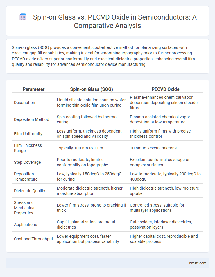
Spin-on glass (SOG) provides a convenient, cost-effective method for planarizing surfaces with excellent gap-fill capabilities, making it ideal for smoothing topography prior to further processing. PECVD oxide offers superior conformality and excellent dielectric properties, enhancing overall film quality and reliability for advanced semiconductor device manufacturing.
Table of Comparison
| Parameter | Spin-on Glass (SOG) | PECVD Oxide |
|---|---|---|
| Description | Liquid silicate solution spun on wafer, forming thin oxide film upon curing | Plasma-enhanced chemical vapor deposition depositing silicon dioxide films |
| Deposition Method | Spin coating followed by thermal curing | Plasma-assisted chemical vapor deposition at low temperature |
| Film Uniformity | Less uniform, thickness dependent on spin speed and viscosity | Highly uniform films with precise thickness control |
| Film Thickness Range | Typically 100 nm to 1 um | 10 nm to several microns |
| Step Coverage | Poor to moderate, limited conformality on topography | Excellent conformal coverage on complex surfaces |
| Deposition Temperature | Low, typically 150degC to 250degC for curing | Low to moderate, typically 200degC to 400degC |
| Dielectric Quality | Moderate dielectric strength, higher moisture absorption | High dielectric strength, low moisture uptake |
| Stress and Mechanical Properties | Lower film stress, prone to cracking if thick | Controlled stress, suitable for multilayer applications |
| Applications | Gap fill, planarization, pre-metal dielectrics | Gate oxides, interlayer dielectrics, passivation layers |
| Cost and Throughput | Lower equipment cost, faster application but process variability | Higher capital cost, reproducible and scalable process |
Introduction to Spin-on Glass and PECVD Oxide
Spin-on Glass (SOG) is a liquid dielectric material applied through spin coating and cured to form a silica-based insulating layer, commonly used for planarization and gap filling in semiconductor fabrication. Plasma Enhanced Chemical Vapor Deposition (PECVD) Oxide deposits silicon dioxide at low temperatures using plasma energy, enabling conformal coatings with precise thickness control for advanced electronic devices. Your choice between SOG and PECVD Oxide depends on factors like application requirements, thermal budget, and desired film properties.
Process Overview: How Spin-on Glass Works
Spin-on Glass (SOG) is a liquid chemical oxide applied directly onto semiconductor wafers through a spin coating process that ensures uniform thin film distribution. The wafer is spun at high speeds to spread the SOG material evenly across its surface, followed by a curing step that solidifies the film into a silicon dioxide layer. This technique offers precise thickness control and excellent planarization, making it suitable for filling gaps and smoothing surfaces in microelectronics fabrication.
Process Overview: Understanding PECVD Oxide
PECVD oxide is a thin film deposited using Plasma Enhanced Chemical Vapor Deposition, involving chemical reactions of silane and oxygen at low temperatures to form a uniform oxide layer. This process provides excellent step coverage and conformality, making it ideal for complex semiconductor device structures. Your choice of PECVD oxide ensures better control over film properties compared to spin-on glass, which is applied as a liquid and then baked to form a solid oxide film.
Material Properties Comparison
Spin-on glass (SOG) exhibits excellent gap-filling capabilities with a low dielectric constant typically around 3.2 to 3.8, making it ideal for planarization and insulation in microelectronics. PECVD oxide films offer superior mechanical strength and thermal stability with a dielectric constant close to 4.0, supporting high-quality passivation and moisture resistance. The choice between SOG and PECVD oxide depends on specific application requirements, balancing dielectric properties, film density, and process compatibility.
Advantages of Spin-on Glass
Spin-on Glass (SOG) offers superior gap-fill capabilities compared to PECVD Oxide, making it ideal for planarizing surfaces with high aspect ratio features. Its low-temperature processing reduces thermal budget constraints, protecting temperature-sensitive substrates and devices. SOG layers also exhibit lower dielectric constants, which enhances device performance by reducing parasitic capacitance in semiconductor applications.
Benefits of PECVD Oxide Deposition
PECVD oxide deposition offers superior uniformity and conformality compared to spin-on glass, ensuring consistent coverage over complex topographies. This method provides lower defect densities and better integration with semiconductor processes, resulting in enhanced electrical performance and reliability. You benefit from improved film quality and precise thickness control, critical for advanced microelectronics and MEMS applications.
Limitations and Challenges of Both Techniques
Spin-on glass (SOG) faces challenges such as limited film thickness uniformity and potential contamination during the curing process, which can affect dielectric reliability. PECVD oxide presents issues with higher film stress and lower density compared to thermal oxides, leading to potential cracks and reduced electrical performance. Both techniques require careful process optimization to balance deposition parameters, film quality, and integration compatibility in semiconductor fabrication.
Application Areas: When to Choose Each Method
Spin-on glass (SOG) is ideal for planarizing surface topographies in microelectronics and semiconductor fabrication, especially where low-temperature processing is required to protect sensitive underlying layers. PECVD oxide excels in high-quality dielectric layer deposition with excellent conformality and control over thickness, making it suitable for advanced integrated circuit insulation, passivation, and MEMS applications. Your choice depends on whether surface smoothness or precise, uniform oxide films are critical to your device performance and process compatibility.
Cost and Scalability Considerations
Spin-on glass offers lower initial costs and simpler application processes compared to PECVD oxide, making it cost-effective for small-scale production or prototyping. PECVD oxide, while more capital-intensive due to equipment and process complexity, provides superior uniformity and better scalability for large-volume semiconductor manufacturing. Your choice depends on balancing budget constraints with the need for high-throughput and consistent film quality.
Future Trends in Dielectric Film Deposition
Future trends in dielectric film deposition emphasize the integration of spin-on glass (SOG) and plasma-enhanced chemical vapor deposition (PECVD) oxide to achieve superior film uniformity and low dielectric constant properties. Advances in SOG formulations are targeting enhanced gap-fill capabilities and reduced thermal budgets, while PECVD developments focus on increasing deposition rates and controlling film stress for next-generation semiconductor devices. Emerging hybrid techniques combining spin-on and PECVD processes promise to optimize dielectric performance for 5G, AI chips, and flexible electronics manufacturing.
Spin-on Glass vs PECVD Oxide Infographic